Researchers at Rice University have developed a new way to create nanoscale patterns directly on chip materials at room temperature.
The method uses a stressed crystal and an electron beam to form tiny ripple structures on hard materials such as silica. Scientists say the process can simplify the production of future photonic and optoelectronic devices that use both light and electricity.
Crystal Stress Chips Patterns
The research team used a material called alpha-molybdenum trioxide, which is a semiconducting crystal with directional properties. This feature is known as anisotropy. It means the material reacts differently depending on the direction of the force acting on it. That unique behavior allowed researchers to guide stress in a controlled way.
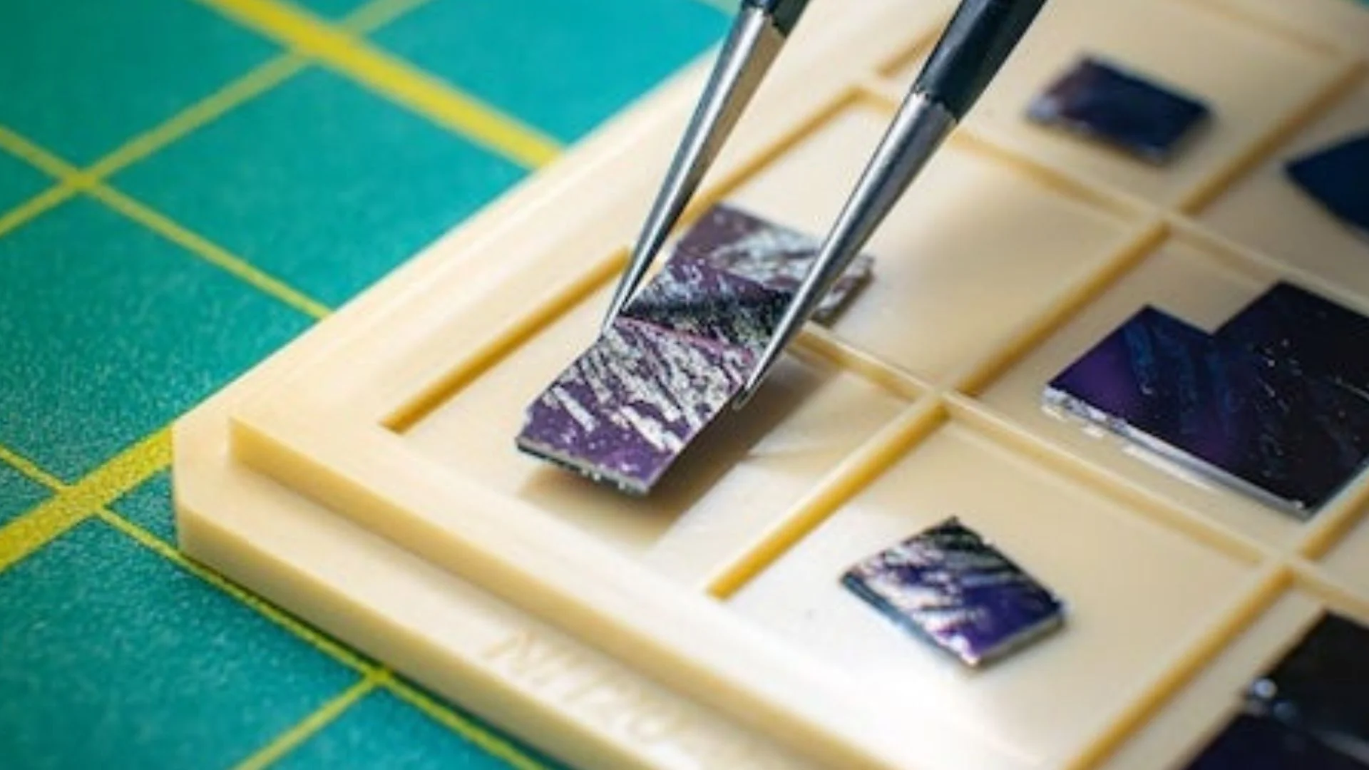
The scientists placed a thin layer of the crystal on top of silica, a common material used in chips and electronic devices. They then exposed the layered material to an electron beam. The beam caused the crystal layer to deform and buckle, while also softening the silica underneath.
As the stress spread across the surface, the materials formed evenly spaced nanoscale ripples. These ripple patterns aligned with the crystal’s internal atomic structure. The process created organized structures without using traditional high-temperature manufacturing methods.
READ ALSO: GE Vernova Acquires Robotech Automation to Modernize Energy Manufacturing Operations
The study was published in the journal Nature Communications. Researchers said the entire patterning process happens in a single step and at room temperature. That removes the need for multiple chemical treatments and expensive fabrication stages.
How Electron Beam Changes Material
According to assistant professor Hae Yeon Lee, silica alone does not naturally deform under an electron beam. However, its atomic bonds can slowly rearrange when exposed to the beam. The challenge was finding a reliable source of stress strong enough to shape the material.
The alpha-molybdenum trioxide layer solved that problem by acting as the stress source. Under the electron beam, the crystal generates directional surface stress. This force translated atomic-scale crystal behavior into ripple patterns hundreds of nanometers wide.
The structures are extremely small compared to a human hair. Yet they can still manipulate light in useful ways. Researchers compared the effect to the grooves on a compact disc that create rainbow reflections.
These ripple structures act as optical gratings, components that guide and split light on a chip. Optical gratings are important for photonic systems used in communications, sensors, and computing. Devices that use light signals rather than just electrical signals can process data faster and use less energy.
WATCH ALSO: SpaceX is gearing up to conduct 11th flight test of Starship on October 13
Why New Chip-Making Method Matters
Traditional nanoscale patterning often requires several manufacturing stages, clean-room processing, and chemical treatments. Those methods are expensive and can leave unwanted residues on chip surfaces. They also usually depend on softer materials that are easier to deform.
Hard insulating materials, such as silica, tend to crack when engineers try to create wrinkle-like patterns on them. That limitation has made wrinkle-based manufacturing difficult for semiconductor applications. The Rice team showed that controlled wrinkle formation is possible even on rigid materials.
Researchers also tested the same process on aluminum oxide and silicon nitride. Both materials are widely used in semiconductor manufacturing and electronic devices. The results suggest the method can work across several common chip materials.
Another important advantage is tunability. Scientists can adjust the ripple size and pattern by varying the crystal layer thickness or the electron beam strength. This gives engineers more control when designing optical components for advanced devices.
After the process is complete, the crystal layer can simply be peeled away from the silica surface. That leaves behind the patterned structure without additional processing. The simpler workflow could help reduce manufacturing complexity and production costs.
READ ALSO: China Prepares Older Carriers to Deploy J-35 Stealth Fighter Across Full Naval Fleet
The technology arrives as chipmakers search for better ways to integrate photonics into electronics. Modern data centers, artificial intelligence systems, and high-speed communication networks all require faster and more energy-efficient data transfer. Light-based chips are seen as an important part of that future.
Researchers believe the new room-temperature technique offers a practical path toward creating optical structures directly on standard semiconductor materials.