Swiss Cluster, a technology startup originating from the Swiss research institute Empa, has received the 2026 Swiss Economic Award in the Production/Industry category.
The company was recognized for developing advanced equipment that produces highly durable thin-film coatings for a wide range of industrial applications. The award highlights the startup’s ability to transform scientific research into successful commercial products.
The company is based in Spiez, a town located on the shores of Lake Thun in Switzerland. While the region is known for its scenic alpine surroundings, it is also home to growing high-tech innovation. Swiss Cluster has become one of the country’s emerging technology companies by focusing on advanced coating solutions.
Swiss Cluster was founded in late 2020 by materials scientist Carlos Guerra and electronics engineer Kevin Lücke. Both researchers previously worked at Empa’s Mechanics of Materials and Nanostructures laboratory in Thun. Their research focused on strengthening, durabilizing, and better-suiting thin-film coatings for demanding industrial environments.
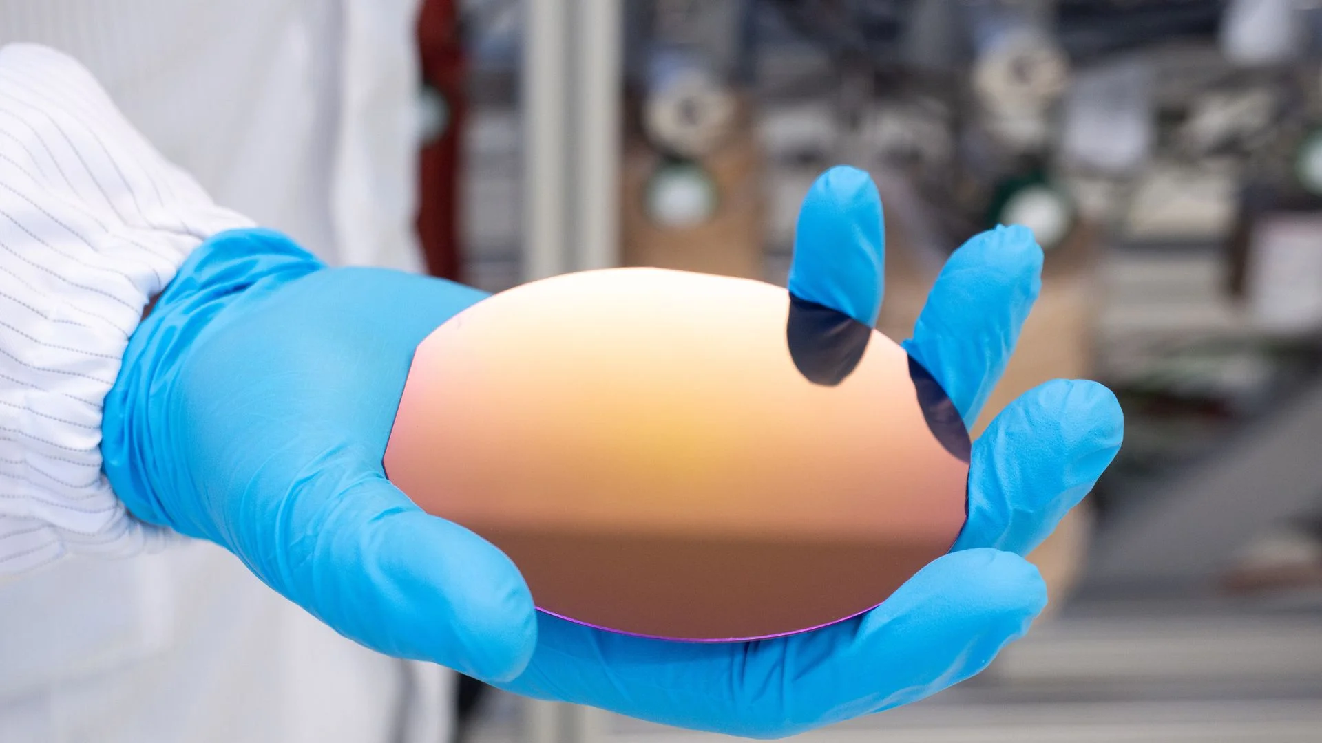
Thin films play an important role in many industries today. They protect components from wear, corrosion, and oxidation while improving performance and lifespan. These coatings are also used in optics, medical devices, watches, batteries, displays, and semiconductor manufacturing.
One of the most important applications of thin-film technology is in electronics. Modern computer chips, transistors, and display systems rely on layers that are often only a few nanometers thick. The quality and precision of these layers directly affect product performance.
READ ALSO: Solid-state battery road tests begin.
Combining Two Coating Tech
Swiss Cluster combines two advanced coating methods in a single system. The first process is Physical Vapor Deposition(PVD). In this method, materials such as metals are vaporized inside a vacuum chamber and then deposited onto a component’s surface.
The second process is Atomic Layer Deposition(ALD). This technique uses gaseous materials that react chemically on a surface to build extremely thin coating layers layer by layer. The process allows manufacturers to control thickness with atomic-level precision.
Each technology offers unique advantages. ALD produces highly uniform coatings that offer excellent corrosion and oxidation resistance. PVD produces hard protective layers that improve durability and wear resistance.
Swiss Cluster’s innovation lies in combining both technologies within a single vacuum environment. This approach prevents contamination that can occur when components are moved between separate machines. Maintaining a continuous vacuum helps improve coating quality and layer adhesion.
The idea emerged from challenges faced during research projects at Empa. Early experiments required researchers to manually transfer materials between separate ALD and PVD chambers while preserving vacuum conditions. The process was time-consuming and difficult to scale.
READ ALSO: Royal Navy duo play pivotal role in trials to arm F-35 jets with UK’s Meteor missile
To solve this problem, the founders developed a machine that integrated both technologies into one system. The new design dramatically reduced production time for complex nanolayer structures. Tasks that previously took about a week in the laboratory could be completed within hours.
Although combined ALD-PVD systems already exist in parts of the semiconductor industry, the Swiss Cluster targets a broader market. The company focuses on sectors such as watchmaking, optics, medical technology, batteries, and industrial manufacturing. This strategy allows the startup to serve customers who often lack access to specialized semiconductor-grade equipment.
Swiss Cluster also offers a separate system designed for batch ALD processing. This technology enables multiple parts or large components to be coated simultaneously. The approach improves efficiency and helps lower processing times for industrial users.
According to the company, atomic layer deposition has been used commercially for only about two decades. However, demand for precise and durable coatings continues to grow across many sectors. As products become smaller, more complex, and more performance-driven, advanced coating technologies are becoming increasingly important.
A key advantage of Swiss Cluster’s systems is accessibility. Unlike many large semiconductor manufacturing tools, the company’s machines are compact and easier to install and operate. This allows research institutions and industrial companies to adopt advanced coating technologies without major infrastructure investments.
The company also operates its own coating laboratory in Spiez. Customers can test coating solutions and evaluate performance before investing in equipment. This service helps companies identify suitable coating technologies while giving the Swiss Cluster valuable feedback for future development.
Since its launch, Swiss Cluster has expanded steadily through equipment sales and service contracts. The company started with an active customer from its earliest days and grew largely through its own revenues. Its first external investment arrived in 2025, several years after its founding.
WATCH ALSO: Boston Dynamics Atlas humanoid robot demonstrates remarkable mobility, balance
Today, Swiss Cluster employs 15 people and works with partners worldwide. Its systems are already installed in research institutions and industrial facilities in Switzerland, the US, and the UK. New deliveries are also planned for France, Italy, Brazil, and China.
The Swiss Economic Award jury praised the company for combining scientific expertise, industrial understanding, and strong execution. The recognition reflects the growing importance of advanced materials and manufacturing technologies in the global industry.
As demand for stronger, smarter, and more precise materials increases, Swiss Cluster is positioning itself as a key supplier of next-generation coating solutions worldwide.