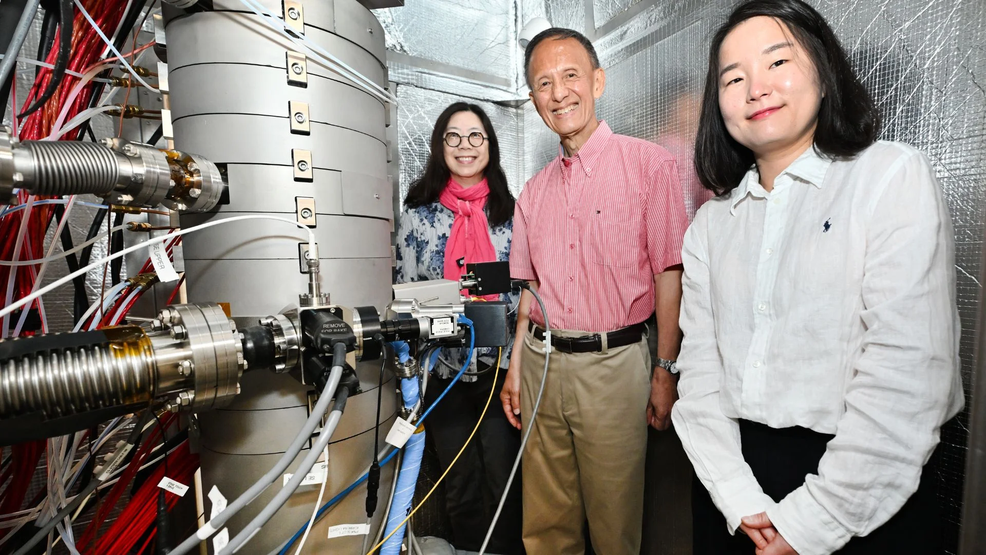
The US Department of Energy’s Brookhaven National Laboratory has added a new scanning transmission electron microscope to its Center for Functional Nanomaterials (CFN).
The advanced instrument was specially designed to strengthen the laboratory’s research capabilities across multiple scientific fields. It is expected to support studies involving energy technologies, quantum materials, microelectronics, and several other advanced research areas.
The microscope complements CFN’s existing collection of electron microscopes and works alongside the X-ray research facilities at the National Synchrotron Light Source II (NSLS-II).
Both facilities operate as user centres supported by the US Department of Energy’s Office of Science. Scientists from universities, research institutes, and industry regularly use these facilities to study materials that are difficult to analyse with conventional methods.
X-ray beamlines have long helped researchers investigate materials at extremely small scales. They reveal valuable information about a material’s internal structure and behaviour that many other techniques cannot detect. Recent advances in electron microscopy now allow similar investigations while providing even greater atomic-level detail.
Designed For Precision Research
The newly installed microscope brings several advanced capabilities into a single research platform. Instead of relying on multiple instruments for different measurements, scientists can study a material’s structure, chemistry, and electronic behaviour using one system. This integrated approach saves time while providing a more complete understanding of complex materials.
Yimei Zhu, leader of Brookhaven Lab’s Advanced Electron Microscopy and Nanoscale Structure and Structural Defects group, said the project fulfilled a long-standing scientific goal.
READ ALSO: ORNL to Lead Nine DOE Genesis Mission Projects Driving AI, Fusion and Future US Science
He said researchers wanted to bring capabilities normally associated with large synchrotron X-ray facilities into an electron microscope. Zhu referred to Professor L. M. Brown’s vision of creating a synchrotron in a microscope and said the new instrument moves closer to that objective.
One of the microscope’s most significant additions is its dual secondary electron detector system. These detectors can simultaneously examine both the upper and lower surfaces of a sample while maintaining atomic-level resolution. Traditional transmission electron microscopes generally focus on internal structures and provide much less information about both exposed surfaces at the same time.
This feature is particularly valuable for catalyst research. Catalysts help speed up chemical reactions and play an important role in energy production, fuel generation, batteries, and industrial manufacturing. By examining both sides of a catalyst before and after a chemical reaction, researchers can better understand how structural changes affect its performance.
Judith Yang, leader of the Electron Microscopy group at CFN, said the new instrument allows scientists to observe these changes in much greater detail.
She explained that comparing catalyst structures before and after reactions provides a clearer picture of how chemical performance changes over time. Such information may help researchers design more efficient materials for future energy systems.
Brookhaven’s Electron Microscope Breakthrough
The microscope also includes major improvements to Electron Energy-Loss Spectroscopy(EELS). This technique measures how much energy electrons lose after passing through a sample. Those energy losses reveal valuable information about a material’s chemical composition and electronic properties.
The upgraded optical system increases the measurable energy range by more than five times compared with previous designs. This wider range enables researchers to investigate additional electronic behaviours and study transition metal elements more effectively. These materials are widely used in batteries, electronics, and advanced manufacturing.
Scientists can also use the upgraded EELS system to examine oxidation states inside materials. Oxidation states describe how atoms exchange electrons during chemical reactions. Monitoring these changes helps researchers understand how batteries charge and discharge, how chemical bonds evolve, and why materials perform differently over time.
Another important feature is a highly advanced energy filtering system. According to Brookhaven Lab, this system delivers an energy resolution around 200 times better than existing microscopes. The higher resolution enables momentum-resolved EELS, allowing scientists to investigate extremely small energy interactions inside materials.
These interactions involve quasiparticles such as phonons, magnons, plasmons, and electronic excitations. Although these names sound complex, they describe different ways energy, heat, light, electricity, and magnetism move through a material. Understanding these processes is essential for designing faster electronic devices, more efficient energy systems, and future quantum technologies.
READ ALSO: These 3D-Printed Bioplastic Pods Could Save Thailand’s Dying Seagrass Meadows
Quantum materials have attracted growing attention because they display unusual physical properties that are difficult to observe using traditional materials. Many researchers believe these materials will support future computing, sensing, and communication technologies. Studying them requires instruments capable of capturing atomic-scale details with exceptional accuracy.
Lower Voltage Imaging Benefits
Another distinguishing feature of the microscope is its ability to operate across a much wider voltage range. Most modern electron microscopes work between 100 and 300 kiloelectron-volts, commonly abbreviated as keV. The new instrument can operate at just 20 keV while still maintaining atomic-scale imaging performance.
Lower operating voltages reduce the risk of damaging delicate samples during examination. This is especially important for two-dimensional quantum materials that may consist of only one or a few layers of atoms. These materials often lose their properties if exposed to higher-energy electron beams for extended periods.
Zhu said the lower voltage design was intentionally developed for sensitive materials research. He explained that lower-energy electrons scatter more effectively while causing less damage to fragile samples. This allows researchers to capture detailed images without significantly altering the materials they are studying.
Many of the microscope’s individual capabilities previously required experiments at specialised X-ray beamlines. Bringing those techniques together inside one electron microscope gives scientists greater flexibility when planning experiments. Researchers can now compare observations from electron microscopy and X-ray facilities more efficiently to build a fuller understanding of complex materials.
Sooyeon Hwang, who helped acquire the microscope before joining Dongguk University as an associate professor, highlighted another advantage of electron microscopy.
She said even the most advanced X-ray imaging techniques generally achieve spatial resolutions measured in tens of nanometres. Modern electron microscopes, by comparison, provide information at the atomic scale.
Supporting Future Discoveries Ahead
Yang described the arrival of the instrument as the beginning of a new period for electron microscopy research. She compared the microscope’s capabilities with the well-known story of blind scientists trying to identify an elephant by touching only one part of its body. Yang said the new system allows researchers to observe much more of the complete picture instead of relying on separate pieces of evidence.
The microscope is expected to attract researchers from many scientific disciplines. CFN welcomes users from universities, national laboratories, and industry who submit research proposals for access to specialised equipment. The expanded capabilities will allow the centre to support new types of experiments that were previously difficult or impossible to perform.
READ ALSO: Samsung, Broadcom Deepen AI Chip Partnership With $200 Billion Semiconductor Expansion
The system also introduces more accessible software based on the Python programming language. The software supports remote operation and creates opportunities for machine learning and automated electron microscopy. These features can help researchers conduct experiments more efficiently while handling increasingly complex datasets.
Hwang said the instrument opens entirely new opportunities for scientific research. She noted that many future experiments will explore questions that researchers previously could not investigate using available equipment. The full scientific impact will become clearer as visiting researchers begin using the microscope for a wide variety of projects.
Brookhaven National Laboratory plans to further strengthen its capabilities with the arrival of a second new electron microscope in the near future. Together, the two instruments will expand the laboratory’s ability to support cutting-edge research across materials science, electronics, energy, and quantum technologies.
As demand for atomic-scale research tools continues to grow worldwide, these investments position CFN to play an increasingly important role in developing the materials that will support future scientific and technological advances.