A team of scientists has identified a simpler and less expensive way to produce one of the world’s rarest forms of silicon.
The research combines advanced experiments with computer modeling to create R8 silicon using lower pressure than traditional methods. The discovery opens new opportunities for energy storage, battery technology, and next-generation electronics while reducing the cost and complexity of manufacturing.
R8 Silicon Production
Silicon is one of the most abundant elements on Earth, after oxygen. It plays a major role in electronics, solar panels, computer chips, and many types of batteries. Scientists have long searched for better forms of silicon that offer improved performance without increasing production costs.
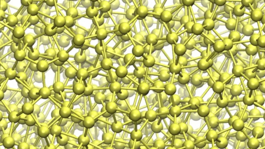
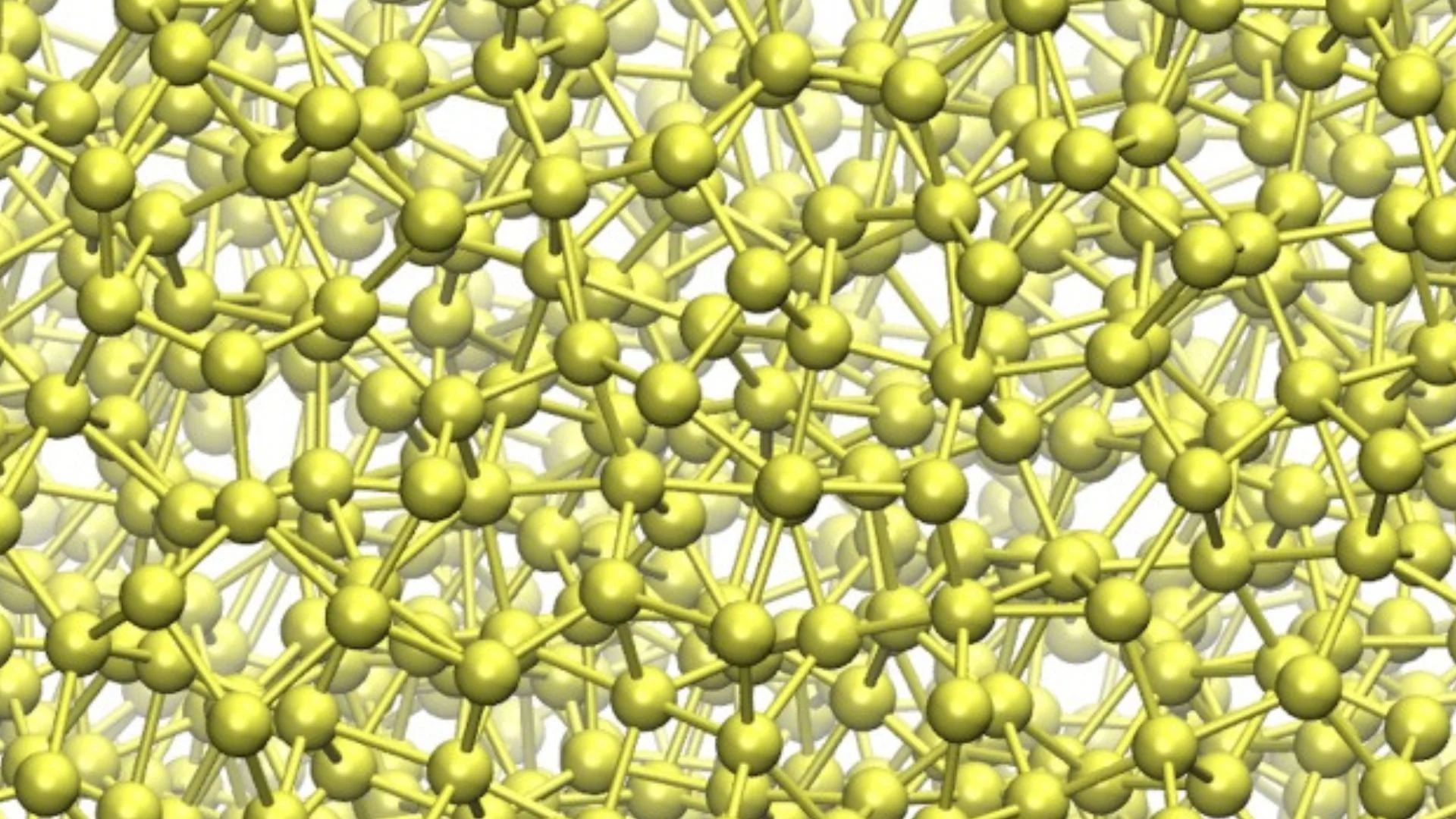
One of those materials is R8 silicon, a rare crystal structure that does not exist naturally. Until now, researchers produced it only inside laboratories by squeezing ordinary crystalline silicon under extremely high pressure. That process required specialized equipment, consumed large amounts of energy, and limited large-scale production.
Researchers from the US Department of Energy’s Oak Ridge National Laboratory worked with international partners to find a simpler solution.
Their study, published in Materials Today, shows that starting with amorphous silicon makes the process much easier. Amorphous silicon has a disordered structure that behaves more like glass than a regular crystal.
Instead of using crystalline silicon, the team compressed amorphous silicon at room temperature. They found that the material transformed into R8 silicon at pressures about 25 percent lower than those used in previous methods. Lower pressure means lower energy use and a simpler manufacturing process.
According to Stephan Irle, a senior computational scientist at Oak Ridge National Laboratory and co-author of the study, researchers spent nearly ten years solving this materials science challenge. He said the new production method offers major energy savings and can be scaled for industrial manufacturing.
How Silicon Changes Structure
The research team wanted to understand exactly how silicon changes during compression. They focused on a scientific principle called density matching. This happens when atoms naturally reorganize into a stable structure once they reach the correct density.
Irle compared the process to building blocks that automatically arrange themselves into the correct pattern. As pressure increases, the disordered atoms in amorphous silicon gradually align into the ordered crystal structure of R8 silicon. This direct transformation avoids several difficult steps required in older methods.
READ ALSO: NASA’s PROMISE Rover: From Mars Spare to Nuclear-Powered Moon Explorer
Scientists observed these changes using powerful research facilities in the US. They carried out neutron diffraction experiments at the Spallation Neutron Source at Oak Ridge National Laboratory. They also used X-ray diffraction at Argonne National Laboratory’s Advanced Photon Source to monitor the structural changes as they happened.
Neutron diffraction and X-ray diffraction allow scientists to examine how atoms move inside materials. These techniques provide detailed information without damaging the sample. The measurements helped researchers confirm every stage of the silicon transformation.
The team also relied on advanced computer simulations. Researchers used Oak Ridge National Laboratory’s Compute and Data Environment for Science high-performance computing system to test different models and compare the results with experimental observations. The simulations verified that the new process accurately explained the material’s behavior.
Gang Seob Jung, a research scientist at Oak Ridge National Laboratory and co-author of the study, said the modeling work played a central role in confirming the findings. The digital analysis helped identify the most accurate approach for understanding the different forms of silicon during compression.
Why the Discovery Matters
The study showed that amorphous silicon offers greater structural flexibility than ordinary crystalline silicon. Because its atoms are not locked into a rigid arrangement, they can reorganize more easily under pressure. This allows the material to enter the R8 crystal structure directly, bypassing several intermediate metallic phases.
Reducing the number of processing steps can simplify manufacturing and lower production costs. It can also improve efficiency by reducing energy consumption during material synthesis. These advantages make the method attractive for industries developing advanced electronic components and battery technologies.
Silicon is already an important material in modern batteries because it stores electrical energy efficiently while remaining relatively inexpensive. R8 silicon offers additional advantages due to its unique crystal structure. Producing it more efficiently could support the development of higher-performance energy storage systems and future electronic devices.
WATCH ALSO: Chinese firm’s humanoid robot can perfectly pick up tennis ball
The researchers also tested the same density-matching principle on germanium. Germanium belongs to the same family of elements as silicon and is widely used in fiber-optic communication systems, infrared devices, and specialized electronics. The successful demonstration suggests that the approach extends beyond a single material.
Scientists believe similar production methods can be explored for other advanced materials used in technology and industry. Expanding the technique to additional materials could simplify manufacturing across several sectors. That would increase the value of this research beyond silicon alone.
The international research team included scientists from Oak Ridge National Laboratory, Australian National University, Argonne National Laboratory, and Lawrence Livermore National Laboratory. Bianca Haberl of Australian National University, who previously worked at Oak Ridge’s Spallation Neutron Source, led the study.
The project received support from the US Department of Energy Office of Science, the National Nuclear Security Administration, the National Science Foundation, and the Australian Research Council. The Spallation Neutron Source and Advanced Photon Source, both operated as US Department of Energy user facilities, provided the advanced instruments required for the research.
This new approach provides scientists with a practical path to produce rare forms of silicon with less energy and simpler manufacturing steps.
As research continues, the same method may be extended to other important materials, helping accelerate future advances in batteries, electronics, and high-performance technologies worldwide.