A team of researchers from Zhejiang University and RMIT University has developed a compact imaging chip that allows cameras to capture more detailed information about the world around them.
The new device helps imaging systems analyze different wavelengths of light directly on the sensor. This enables cameras to identify details that are often invisible in conventional color images.
The research was published in the journal Nature Electronics. The project combines expertise in nanotechnology, photonics, and advanced manufacturing. Scientists say the technology creates a new way to merge imaging and light analysis into a single compact system.
Modern cameras are excellent at capturing visual scenes. However, many industrial and scientific applications require more than standard images. They need information about how materials interact with different wavelengths of light.
This type of analysis is known as spectral imaging. It helps identify materials, detect surface changes, and monitor environmental conditions. Two objects that look identical in a regular photograph can show clear differences when their light signatures are examined.
Traditionally, obtaining this information has required separate and often bulky instruments. Specialized equipment is commonly used in laboratories, factories, and research facilities. These systems can be expensive and difficult to integrate into compact devices.
The newly developed chip addresses this challenge by performing light analysis directly within the imaging hardware. Instead of sending light to external instruments for processing, the chip separates and processes light near the camera sensor. This creates a more compact and efficient sensing solution.
READ ALSO: Iran’s Cluster Missile Warheads: Why the Sky-Splitting Weapon Is So Dangerous
Compact Imaging Chip’s Core Innovation
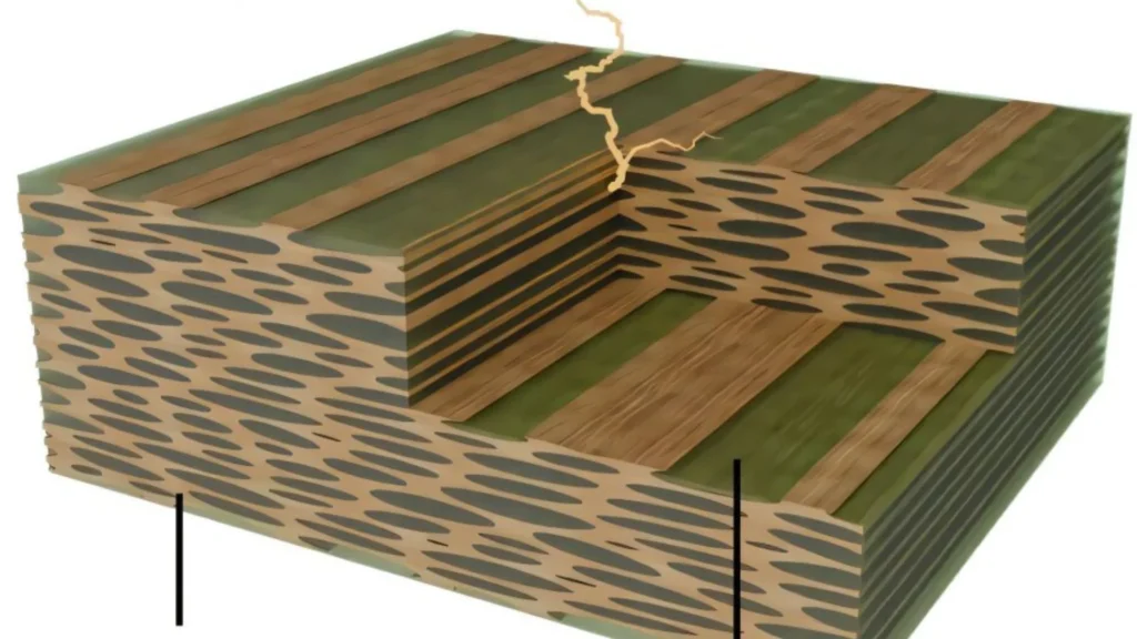
The key innovation lies in tiny spiral-shaped structures created inside transparent materials. Researchers used ultrafast laser pulses to build these microscopic structures with extremely high precision. Each structure acts as a miniature light sorter.
When light enters the device, the structures separate different wavelengths into distinct patterns. An image sensor then reads these patterns and extracts spectral information. This process allows the system to identify characteristics that standard cameras cannot detect.
The technology works across both visible and near-infrared wavelengths. Near-infrared light is commonly used in environmental monitoring, industrial inspection, and scientific imaging. Supporting both wavelength ranges expands the system’s potential applications.
Another advantage is its resistance to changes in viewing angle. Many microscale optical technologies lose performance when the angle of incoming light changes. The new design maintains reliable operation under a wider range of conditions.
Professor Baohua Jia from RMIT University’s Centre for Atomaterials and Nanomanufacturing said the development introduces a new physical component rather than relying solely on software processing.
According to Jia, the system separates light at a microscopic scale close to the sensor. This allows important information to be captured during imaging rather than reconstructed later.
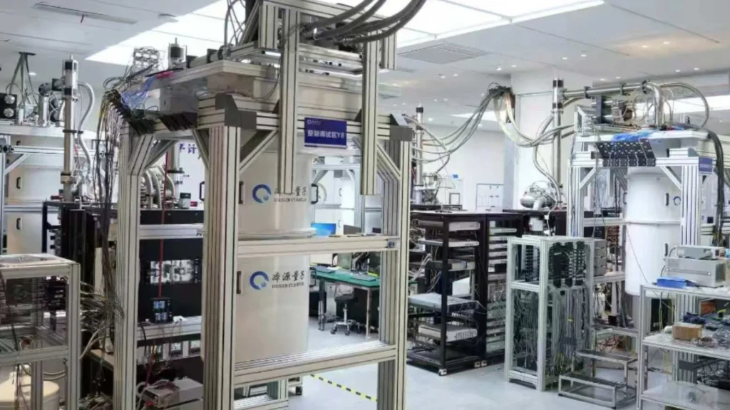
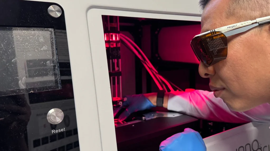
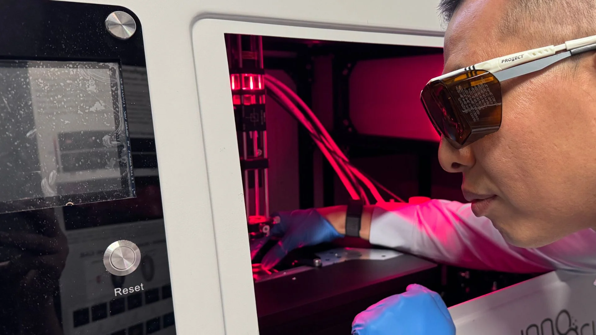
To test the concept, the research team integrated the light-sorting structure with a commercial image sensor. The prototype successfully collected spectral information and demonstrated microscopic spectral imaging capabilities. This proved that the design can function within a real imaging system.
READ ALSO: Israeli F-16 Spotted With Strange Precision Bomb, Experts Suspect Incendiary Weapon
The collaboration involved researchers from Zhejiang University and RMIT University. Professor Jianrong Qiu led the Zhejiang University team, while RMIT contributed expertise in nanomanufacturing, optical characterization, and device testing. Dr. Han Lin, Bo Zhang, and Zhuo Wang also played key roles in the project.
RMIT’s advanced nanofabrication facilities helped researchers create and study structures that are about 1,000 times smaller than a human hair. Such precision is essential for controlling how light behaves at microscopic scales. The facilities enabled rapid testing and design refinement.
Scientists emphasize that the technology is still in its early stages of development. It is not yet a commercial product ready for widespread deployment. Further work is needed before it can be manufactured on a large scale.
The next phase of research will focus on scaling up production methods. Researchers also plan to test additional materials and improve the software used to reconstruct light information from sensor data. These improvements are expected to increase performance and efficiency.
WATCH ALSO: Microsoft delivers first large scale production cluster with more than 4,600 NVIDIA GB300 NVL72
The development arrives as demand grows for smarter sensing systems across multiple industries. Advanced cameras are increasingly used in manufacturing, agriculture, environmental monitoring, healthcare, and autonomous machines. Systems that can gather more information without increasing size or complexity are becoming increasingly valuable.
However, the technology could help create a new generation of compact cameras capable of seeing far beyond traditional color images. By combining imaging and spectral analysis in a single device, researchers are laying the foundation for smarter sensors that can better understand the physical world.