
Researchers have demonstrated ballistic electron transport in single-crystalline copper thin films with dimensions similar to those of modern semiconductor interconnects.
The achievement shows that electrons can move through copper with minimal scattering under specific conditions, challenging long-held assumptions about the metal’s limitations.
The findings offer a new perspective on how future chip wiring can be designed to improve speed, efficiency, and energy use.
The results were published in the journal Nature Communications.
Ballistic transport occurs when electrons move through a material without frequently colliding with defects, impurities, or lattice vibrations. In this state, electrons travel along relatively straight paths. This allows electrical signals to move more efficiently through a material.
Scientists have previously observed ballistic transport in materials such as graphene and specially engineered semiconductor structures. However, copper has long been considered an unlikely candidate because its electrons typically scatter frequently. These scattering events increase resistance and reduce electrical efficiency.
Ballistic Electrons Beat Copper
The research team was led by Professor Gil-Ho Lee from POSTECH, Professor Emeritus Se-Young Jeong from Pusan National University, and Professor Seong-Gon Kim from Mississippi State University. Their work focused on creating copper films with extremely high structural quality. The goal was to reduce the factors that normally disrupt electron movement.
READ ALSO: Ukraine’s New AI Drone Defense System Automates 95% of Shahed Interception
To achieve this, the researchers produced single-crystalline copper films using a technique called Atomic Sputtering Epitaxy(ASE). Unlike conventional copper films, these samples contained no grain boundaries. Grain boundaries are microscopic interfaces between crystal regions that often act as barriers to electron flow.
The copper films were grown with a Cu(111) crystal orientation and featured a surface roughness of only about 0.2 nanometers. Such smoothness significantly reduces opportunities for electrons to scatter. The result is a cleaner pathway for electron movement inside the material.
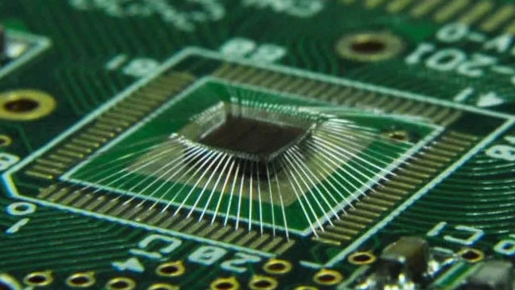
The team tested structures that were about 80 nanometers thick and 150 nanometers wide. These dimensions are particularly important because they are comparable to the widths used in semiconductor chip interconnects. Interconnects are the tiny metal wires that connect billions of transistors inside advanced processors.
In ordinary copper conductors, electron transport follows a diffusive pattern. Electrons repeatedly collide with obstacles as they move through the metal. This behavior creates electrical resistance and contributes to energy loss.
READ ALSO: GE Aerospace and Wolfspeed Team Up to Scale High-Voltage Silicon Carbide Technology
When ballistic transport occurs, electron behavior changes significantly. One key indicator is a phenomenon known as negative bend resistance. This unusual electrical signal appears during specialized nonlocal voltage measurements and serves as evidence that electrons are moving with minimal scattering.
The researchers detected this signature and confirmed the presence of ballistic transport in their copper structures. The measurements were performed at temperatures below 85 Kelvin, which is approximately minus 188 degrees Celsius. These low temperatures help suppress vibrations within the material and make ballistic transport easier to observe.
One of the most significant aspects of the study is the size of the tested structures. Previous demonstrations of ballistic transport often relied on highly specialized materials or laboratory-scale devices. In contrast, this work used copper dimensions that are relevant to real semiconductor manufacturing.
The findings arrive at a time when the semiconductor industry faces growing challenges with interconnect scaling. As chip components become smaller, the resistance of metal wiring tends to increase sharply. This growing resistance can slow signal transmission and generate additional heat.
READ ALSO: World’s largest nuclear fusion research project ITER has reached a new milestone
Reducing resistance has become a major goal for chip designers. Ballistic transport offers a potential route to address this problem because electrons encounter fewer obstacles as they travel through the conductor. In principle, this can lower energy losses and improve overall performance.
The technology also carries implications for power consumption. Lower resistance means less energy is converted into unwanted heat. This can help support the development of faster and more energy-efficient electronic systems.
Professor Lee said ballistic transport represents an ideal transport mechanism for reducing power consumption in electronic devices. He noted that the study’s importance lies in demonstrating this effect in copper, an industry-standard metal, at dimensions relevant to semiconductor interconnects.
While further research is needed to explore practical applications, the study provides new insight into the future of chip design. It shows that copper can exhibit transport behavior once thought impossible for the material.