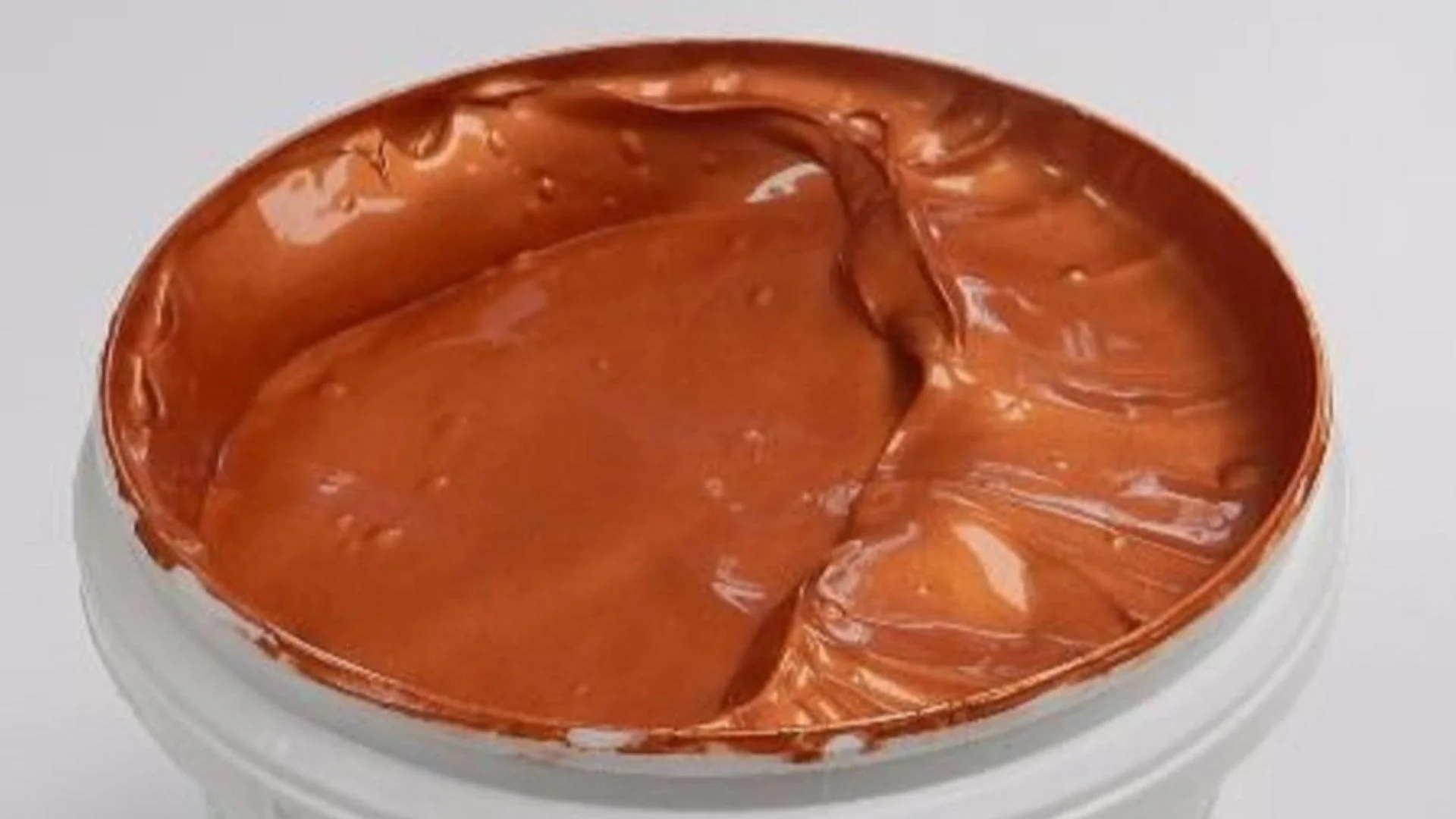
Researchers in the US have developed a new copper ink that can print durable copper structures without the corrosion and oxidation that normally damage the metal.
The innovation enables copper to be printed on a wide range of surfaces while remaining stable over time. Scientists say the technology offers a faster and more cost-effective way to manufacture electronic components.
It also helps reduce material waste compared with conventional production methods. The research was carried out by a team from the University of Maryland, Yale University, and Lawrence Berkeley National Laboratory.
The study was published as a cover article in the journal Science. The project was led by Shenqiang Ren, working alongside Liangbing Hu and Haimei Zheng. Their collaboration spanned more than a decade before achieving the result.
READ ALSO: YASA Shatters Electric Motor Power Density Record With Staggering 59kW/kg Prototype
Copper Ink Defies Corrosion
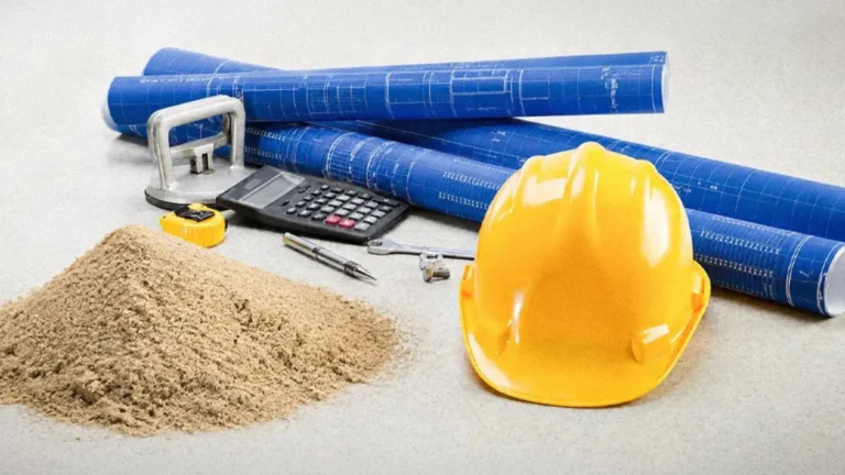
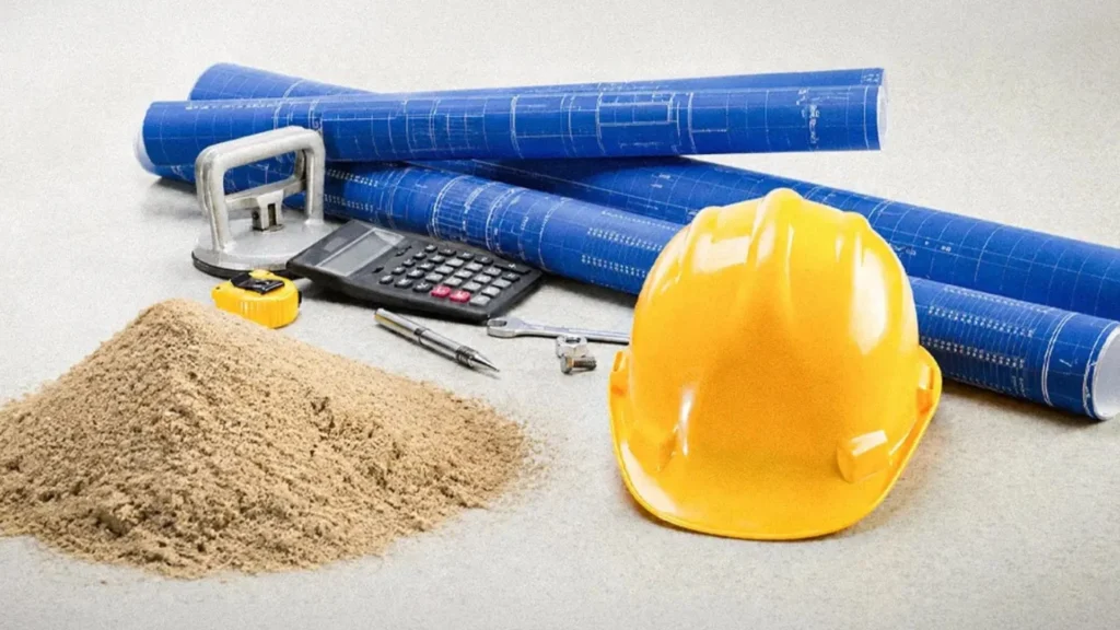
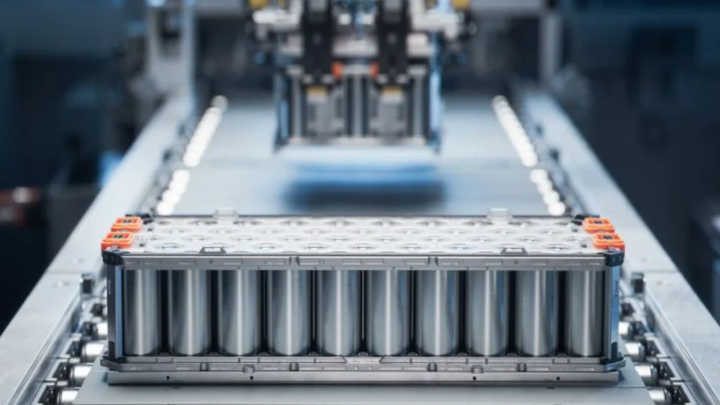
Copper is one of the most widely used metals in modern technology. It powers data centers, artificial intelligence systems, wireless networks, solar panels, batteries, and electronic circuit boards. Keeping copper stable for long periods has remained a major challenge for manufacturers.
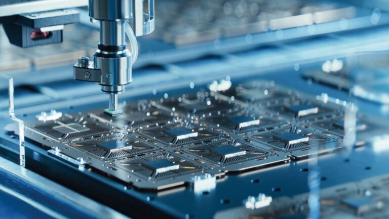
The team developed a blue reactive ink that can be printed under normal conditions. It transforms into copper at a relatively low temperature of about 150 degrees Celsius. This process is simpler than many traditional copper manufacturing methods.
Scientists say the new approach solves two long-standing problems simultaneously. It allows copper inks to be printed easily while also protecting the finished copper from corrosion and oxidation. These improvements can help extend the lifespan of electronic components.
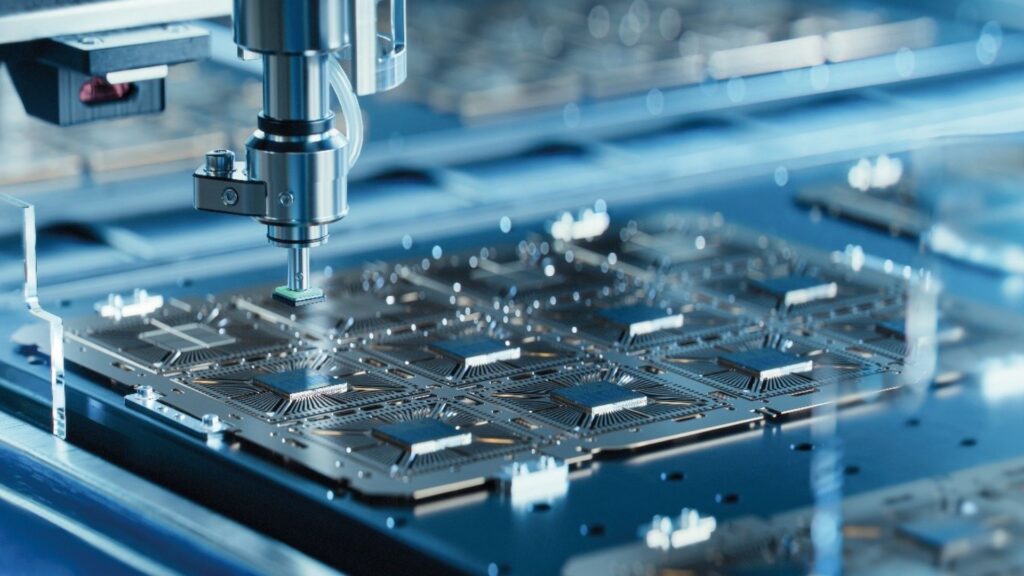
Ren said the printed copper traces serve as wiring inside advanced electronic devices. According to him, the method enables faster production while lowering costs and reducing material waste. This makes the technology attractive for large-scale manufacturing.
Applications From Solar Cells to Seawater Testing
To demonstrate the ink’s versatility, researchers printed copper conductor traces for solar cells and circuit boards. They also produced miniature versions of the University of Maryland’s Testudo statue and models of the Eiffel Tower. These examples showed that the ink can work across different shapes and surfaces.
The team conducted durability tests to assess long-term performance. Copper structures made with the ink remained intact even after six months of submersion in seawater. This result suggests strong resistance to harsh environmental conditions.
The new process offers an alternative to traditional copper plating and chemical etching. These conventional methods often require more time, energy, and chemical use. Replacing them with printed copper production could lower environmental impacts across multiple industries.
READ ALSO: Germany Pitches Type 212CD Submarine to Canada Against South Korea’s Hanwha Ocean Bid
Hu said the technology allows manufacturers to use copper instead of more expensive conductive metals such as silver. This can reduce costs in electronics, energy systems, and environmental technologies. Wider adoption of copper-based conductive inks could make advanced devices more affordable.
The researchers have also launched a startup, NewCopper, to bring the technology to market. As demand for electronics, AI infrastructure, and renewable energy systems continues to grow, durable and low-cost copper printing could play an important role in future manufacturing.