Researchers from Japan and Switzerland have developed a new way to guide spin wave signals through sharp turns with very low energy loss.
The method improves signal transmission more than 5,000 times compared to conventional designs. The discovery supports the development of faster and more energy-efficient computing systems for artificial intelligence and data centers.
A team from Tohoku University, Shin-Etsu Chemical Co., Ltd., and EPFL created the new structure using a special magnetic material and a patterned copper film.
Their work focuses on spin waves, which are tiny magnetic ripples that carry information without moving electric charges. Because they generate far less heat than electrons, spin waves are seen as an important option for future low-power computing.
Modern data centers and AI systems consume large amounts of electricity every day. Traditional computer chips rely on moving electrons through circuits, which generates heat and energy loss. As computing demand worldwide grows, researchers are seeking technologies that can process information more efficiently.
New Crystal Improves Magnonics
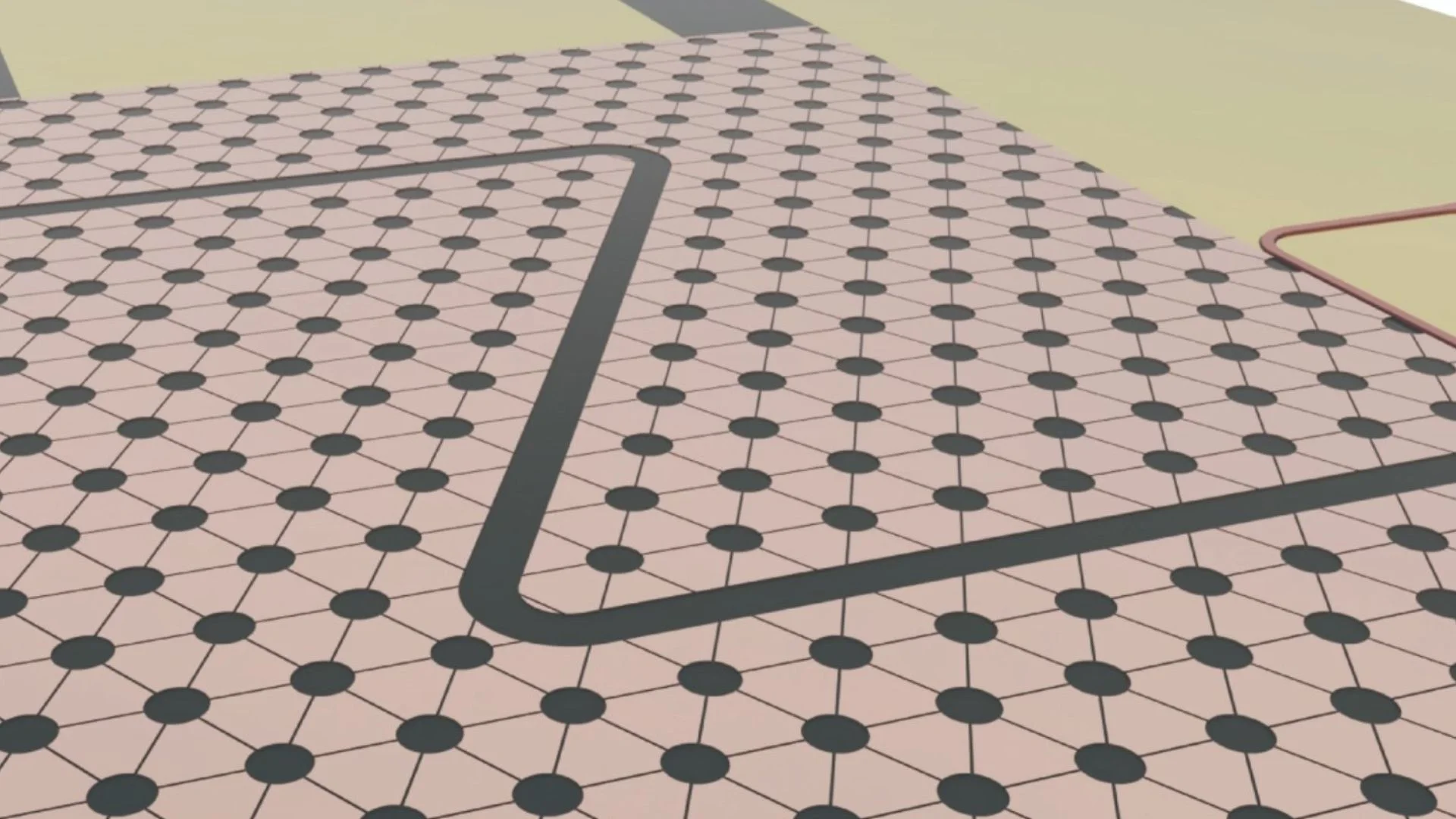
The research team built a two-dimensional magnonic crystal by depositing a copper film on a magnetic garnet layer. The copper film contained a hexagonal pattern of tiny holes connected by narrow slits. This design controlled how spin waves moved through the material.
READ ALSO: Blue Origin Rocket Explosion at Cape Canaveral Puts NASA Moon Plans Under Pressure
Earlier studies by the same team used copper disks on the garnet surface. In the new study, the researchers reversed that concept by creating holes inside a copper film instead. According to the team, this change provided much stronger control over spin-wave motion.
Using three-dimensional electromagnetic simulations, the researchers found that the structure created a complete magnonic bandgap. This bandgap blocks spin waves from traveling in unwanted directions. As a result, the waves remained confined within the designed pathway, resulting in much lower signal loss.
The team said this is the first time a complete magnonic bandgap has been demonstrated in a two-dimensional magnonic crystal based on magnetic garnet. The achievement represents an important step for spin wave engineering. Researchers also confirmed that a patent application has already been filed for the waveguide structure.
Z-Path Unlocks Spin Waves
One of the biggest problems in spin-wave computing has been signal weakening at bends. In conventional waveguides, spin waves lose strength quickly when forced to travel through corners. This has limited the development of practical spin wave circuits for real computing systems.
To solve this issue, the researchers created a Z-shaped path inside the crystal. They formed the path by removing a line of holes from the patterned copper layer. This created a line defect that served as a controlled route for the spin waves.
The results showed a dramatic improvement in signal transmission. Spin waves traveling through the new Z-shaped waveguide remained strong even after sharp turns. In comparison, signals in conventional ridge waveguides faded before reaching the end of the path.
The new design transmitted spin waves more than 5,000 times more effectively than earlier waveguide approaches. That large increase underscores the importance of controlling wave motion within magnetic materials. It also shows how carefully designed structures can solve long-standing engineering problems.
Associate Professor Taichi Goto from Tohoku University explained the significance of the work in a statement.
He said the team solved the problem by placing a patterned metal film on a magnetic garnet instead of cutting the garnet itself. He added that the method allows spin waves to move around sharp corners with minimal loss.
Spin Wave Computing Explained
Spin wave technology is attracting attention because it can process information with far lower energy use than standard electronics. Unlike traditional systems, spin wave devices do not depend on the physical movement of electrons through wires. This reduces heat generation and improves energy efficiency.
WATCH ALSO: India recently tested carried out the successful launch of Intermediate Range Agni-Prime Missile
Lower heat production is especially important for artificial intelligence infrastructure. AI models require massive computing power, and modern data centers already face rising cooling and electricity costs. More efficient hardware designs could help reduce operational expenses and environmental impact.
Researchers worldwide are exploring magnonics as a future computing platform. Magnonics is the field that studies spin waves and their use in data processing. Scientists believe spin wave circuits may eventually support faster communication between chip components while consuming much less energy.
The latest study demonstrates that complex spin-wave paths can operate efficiently within compact structures. This opens the possibility of building integrated spin wave chips for advanced computing applications. It also strengthens efforts to develop alternatives to conventional semiconductor technologies.
The findings were published on May 27, 2026, in the journal Physical Review Applied. The research adds momentum to global work on next-generation low-power computing systems. Future studies will focus on turning these laboratory designs into practical devices for commercial electronics and data center hardware.