Researchers at the University of Texas at Austin have developed a compact EUV lithography printer that could accelerate semiconductor research and make it more affordable.
The new tabletop system creates complex 3D nanoscale patterns in minutes instead of days. The project aims to reduce barriers that have long limited advanced chip manufacturing research.
Semiconductors are essential components used in smartphones, computers, data centers, vehicles, and countless electronic devices. Producing advanced chips requires highly specialized equipment and facilities. These requirements make semiconductor manufacturing one of the most expensive industries in the world.
One of the most important technologies used in modern chip production is extreme ultraviolet lithography. This process uses very short-wavelength light to print tiny circuit patterns onto silicon wafers. Those patterns eventually become the transistors and circuits that power electronic devices.
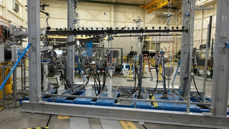
Traditional EUV lithography systems are enormous and extremely expensive. A commercial EUV machine can cost more than $200 million and occupy an entire room. Only a small number of companies globally have the resources to operate such equipment at scale.
READ ALSO: Montreal’s Hidden Climate Culprit: The Surprising Source Choking Our Air
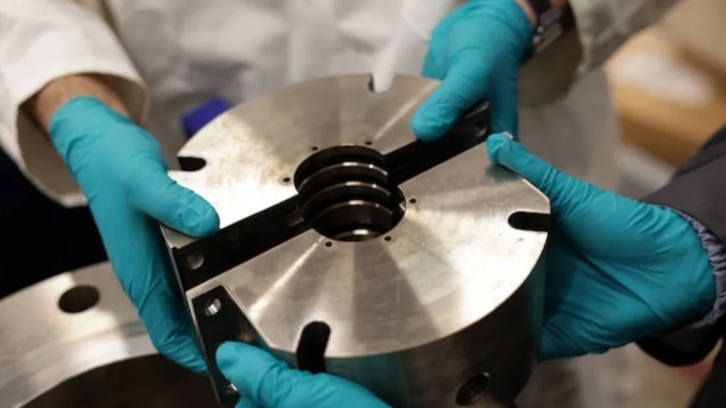
The research team focused on simplifying this process. They removed many of the complex elements from commercial systems and retained only the essential components for research. The result is a modular tabletop printer that is smaller, more flexible, and significantly less expensive.
The new printer works alongside a manufacturing method known as volumetric 3D patterning. This technique allows researchers to create three-dimensional nanostructures in a fundamentally different way. Instead of building structures one layer at a time, multiple layers can be patterned simultaneously.
This difference has a major impact on production speed. Conventional EUV processes often require many separate steps to create 3D structures. While individual printing stages can be quick, the complete manufacturing process often takes several days.
The new approach dramatically reduces that timeline. Researchers reported that pattern exposures now take only minutes. Faster processing enables scientists to test designs more quickly and move research projects forward.
The study was published in the journal Nano Letters. The work was supported by the National Science Foundation Future of Semiconductors (FuSe2) initiative. The program focuses on reducing research costs and expanding access to semiconductor innovation.
Professor Chih-Hao Chang from the Walker Department of Mechanical Engineering helped lead the project. He explained that processing time has been a major limitation in creating advanced 3D semiconductor structures. The new method addresses that challenge by enabling parallel patterning instead of a layer-by-layer approach.
READ ALSO: Russia Tests Nuclear-Powered Burevestnik Missile Amid Ukraine War and Trump Peace Talks
Researchers have already begun testing new EUV-sensitive materials using the tabletop system. These materials were developed by collaborators at the University of Texas at Dallas and Johns Hopkins University. Additional materials are expected to be evaluated as the project continues.
At present, the technology can create periodic structures. These repeating patterns are particularly useful for memory devices and photonic technologies. Photonics uses light instead of electricity to transmit and process information in advanced computing and communications systems.
The researchers plan to further improve the printer. Future versions are expected to support faster operation and more detailed nanoscale features. Smaller and more precise structures could enable higher transistor densities and more powerful chips.
The potential applications extend beyond semiconductor manufacturing. The ability to rapidly create complex 3D nanostructures could support research in medicine, quantum technologies, and advanced materials science. Scientists believe these capabilities could help accelerate development across several high-tech industries.
The project highlights a broader effort to make advanced semiconductor tools more accessible to universities and research institutions. Lower-cost equipment allows more organizations to participate in chip research. Greater access can help speed innovation and strengthen future technology development.
WATCH ALSO: This robotic system to pick strawberries automates tough tasks
As work continues, researchers hope the tabletop EUV platform will become a valuable tool for exploring next-generation semiconductor designs.
Faster testing, lower costs, and improved flexibility could help bring new ideas from the laboratory to real-world applications more efficiently. The technology represents an important step toward expanding access to advanced nanoscale manufacturing and supporting the future of electronics.