
IBM unveils Nanostack, the world’s first sub-1nm chip technology, marking a major leap in semiconductor research and AI computing power.
The new chip is built using a completely new transistor design that allows far more transistors to fit into a tiny space. The company says this technology opens a new chapter in chip development as the industry looks beyond today’s manufacturing limits.
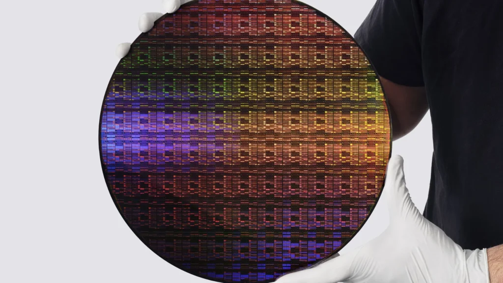
The new processor is built on a 0.7-nanometer process, also known as the 7-angstrom node. IBM says the chip packs nearly 100 billion transistors into an area about the size of a fingernail. That is almost twice the transistor density of the company’s 2-nanometer chip introduced in 2021.
Nanostack Design Chips
The biggest change comes from IBM’s new transistor architecture called Nanostack. Instead of placing transistors only side by side, the new design stacks them vertically in multiple layers. This three-dimensional structure allows engineers to place more transistors in the same chip area without increasing the chip’s size.
Modern chips are reaching physical limits because traditional designs have become extremely small. IBM developed Nanostack to continue shrinking chips while improving their performance. The new design also gives engineers more flexibility when selecting materials for different layers of the chip.
Each stacked layer can use different material combinations depending on its purpose. This helps improve speed, power efficiency, and overall chip performance. It also allows engineers to optimize each transistor layer independently, rather than treating the chip as a single structure.
READ ALSO: New ETH Zurich Pixel Sees and Displays at Once, Redefining How Light Is Used
IBM says the technology has already been tested successfully in several experiments. Researchers demonstrated ultra-thin dielectric bonding, dual-channel engineering, and the operation of a working CMOS inverter. These tests confirm that the architecture can perform real computing tasks rather than remaining only a laboratory concept.
The company also presented additional research during the 2026 Symposium on VLSI Technology and Circuits. According to IBM, the Nanostack design improves SRAM scaling by about 40 percent. SRAM is a type of memory used inside processors for very fast data access during computing tasks.
Better SRAM scaling becomes increasingly important as artificial intelligence models continue growing in size. Faster memory allows processors to move large amounts of data more efficiently. This helps improve performance in AI training, cloud computing, and other demanding workloads.
Target AI and Cloud Computing
IBM projects significant improvements compared with its earlier 2-nanometer technology. The company says future chips based on the new design can deliver up to 50 percent higher performance. They can also provide up to 70 percent better energy efficiency depending on the workload.
Higher performance allows computers to complete complex tasks faster. Better energy efficiency reduces electricity consumption while producing less heat. These improvements are becoming valuable as AI systems require more computing power than ever before.
The technology is expected to benefit many industries beyond artificial intelligence. Advanced processors are used in cloud data centers, smartphones, personal computers, communication equipment, vehicles, industrial automation systems, and key infrastructure. Faster, more efficient chips can improve performance across all these sectors.
IBM Research Director and IBM Fellow Jay Gambetta said the company has moved chip development beyond the nanometer era toward atomic-scale engineering.
READ ALSO: Cornell Students Build Community Bridges Through Engineering Course That Delivers Real Impact
He said the Nanostack design changes how chips are built rather than simply making existing transistors smaller. He added that the architecture creates a foundation for future generations of high-performance computing.
The term sub-1 nanometer does not mean every feature inside the chip measures exactly 0.7 nanometers. Today, manufacturing nodes mainly represent generations of semiconductor technology rather than precise physical dimensions. Even so, IBM says its new design demonstrates that chip scaling can continue below the 1-nanometer level.
IBM Plans Production Within Five Years
IBM believes Nanostack provides a roadmap for at least another decade of semiconductor scaling. The company expects the first commercial adoption of this technology within the next five years. That timeline depends on continued development and manufacturing readiness.
The research is being carried out at IBM’s semiconductor research facility in Albany, New York. The site works closely with industry partners to develop future chip manufacturing technologies. It will soon receive a High Numerical Aperture Extreme Ultraviolet lithography system that enables extremely precise circuit printing.
The advanced lithography machine is being developed by ASML. IBM is also collaborating with Lam Research, Tokyo Electron, and SCREEN Semiconductor Solutions to create new manufacturing processes. The partners have already demonstrated working semiconductor devices using these advanced techniques.
WATCH ALSO: Drum-shaped antenna reflector on NASA-ISRO NISAR satellite deployed
IBM has played a major role in semiconductor research for decades. The company has contributed to several important chip technologies, including its earlier 2-nanometer processor announced in 2021. It continues investing in silicon research alongside artificial intelligence hardware and quantum computing.
The company also recently announced plans to establish Anderon as the world’s first pure-play quantum foundry. The new business will focus on manufacturing quantum wafers, leveraging IBM’s semiconductor expertise. IBM says the initiative aims to strengthen advanced technology manufacturing in the US.
The latest sub-1 nanometer chip demonstrates that semiconductor innovation continues even as devices approach atomic dimensions.
As AI, cloud computing, and high-performance systems demand greater efficiency, IBM‘s new architecture provides a clear direction for the next generation of processors and future computing platforms.