

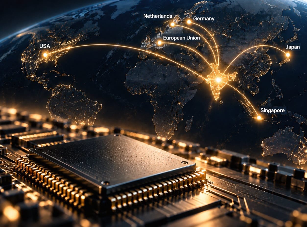
India is moving beyond semiconductor policy announcements and into a phase defined by commercial production, supplier networks and deeper international partnerships.
Prime Minister Narendra Modi opened SEMICON India 2026 in New Delhi on September 17, unveiling Semicon 2.0 as the next stage of the country’s effort to build a complete semiconductor ecosystem. The programme expands support across chip design, manufacturing, advanced packaging, equipment, materials, research and talent.
The fifth edition of SEMICON India runs from September 17 to 19 at Yashobhoomi in New Delhi. More than 600 exhibitors are participating, with roughly half of the companies coming from outside India, while six country pavilions and 12 Indian state pavilions showcase regional and international capabilities.
The event also brings startups, universities and workforce programmes into the same ecosystem, reflecting the industry’s increasingly broad requirements.
READ ALSO: https://modernmechanics24.com/post/idaho-state-university-nuclear-reactor/
The timing is significant for the global semiconductor industry. Chips sit at the centre of artificial intelligence, connected devices, electric vehicles, telecommunications, data centres and modern industrial systems. India is now seeking a larger role across that supply chain, rather than concentrating only on chip design and downstream electronics.
From Approvals To Production
One of the clearest signals at SEMICON India 2026 was the move from approved projects to operating production lines.
PM Modi virtually inaugurated commercial semiconductor production at CDIL Semiconductor in Mohali for discrete devices and at Suchi Semicon in Surat for semiconductor packaging. These facilities bring the number of operational commercial semiconductor ATMP units in India to five, alongside Micron, Kaynes Semicon and CG Semi, from the 12 units approved under Semicon 1.0.
ATMP means assembly, testing, marking and packaging. These processes prepare semiconductor devices for integration into electronic products and are essential links between chip manufacturing and finished systems. India is therefore building capabilities at several stages of the chain rather than relying on a single manufacturing model.
Micron CEO Sanjay Mehrotra said commercial DRAM and NAND production is now live at the company’s Sanand facility in Gujarat.
DRAM is widely used as working memory, while NAND provides the storage used in products such as smartphones, computers and data-storage systems. The start of commercial output gives India’s semiconductor programme a direct connection to the global memory market.
Tata Electronics also reported that construction of its 300mm wafer fab in Dholera and its OSAT facility in Jagiroad remains on track. A wafer fab manufactures semiconductor devices on large silicon wafers, while an OSAT facility handles assembly and testing after fabrication. Together, the projects point to an effort to establish manufacturing and packaging capabilities within the same national ecosystem.
WATCH ALSO: https://modernmechanics24.com/post/ai-robots-physical-ai-real-world/
Semicon 2.0 Widens Scope
The government has positioned Semicon 2.0 as an expansion of the foundation created under the first phase of India’s semiconductor programme.
Union Electronics and IT Minister Ashwini Vaishnaw said Semicon 1.0 established key capabilities, including training for 70,000 design engineers and deployment of electronic design automation tools across more than 500 organisations. The second phase is organised around six pillars: Design, Equipment and Materials, Fabs, Advanced Packaging, Applied R&D and Talent.
The distinction matters because a semiconductor ecosystem is larger than a fabrication plant. A modern fab needs specialised equipment, ultra-pure chemicals, industrial gases, precision components and qualified suppliers operating to demanding standards. It also needs engineers, technicians and researchers who can support production, process development and future chip designs.
India Semiconductor Mission funding is also expanding. Modi said the budget is increasing from USD 8 billion under Semicon 1.0 to USD 13.5 billion for Semicon 2.0. The government has said the first six-year funding phase was committed in four years, accelerating the transition to the next stage of the programme.
The strategy also puts applied research closer to the centre of the semiconductor effort. Universities and research institutions are expected to connect more directly with industry, while talent programmes are designed to create a larger pool of workers with practical semiconductor skills. That combination is important because manufacturing capacity without specialised expertise can limit the development of a sustainable local supply chain.
Global Suppliers Deepen Presence
The announcements from international technology companies show how India’s semiconductor ambitions are drawing investment beyond chipmakers themselves.
Applied Materials announced its “India Vision 2035”, which includes USD 5 billion of investment over the next decade and a tenfold expansion of its India-based supply-chain capacity by 2035. The company supplies equipment used in semiconductor manufacturing, making its planned expansion relevant to India’s efforts to localise more of the production ecosystem.
Lam Research announced an investment of about ₹10,000 crore for its first silicon-component manufacturing and vertical ingot-processing plant in India. The company also said its Semiverse programme has expanded to more than 99 universities. The programme gives students exposure to semiconductor manufacturing through virtual environments and complements the industry’s physical training infrastructure.
Tokyo Electron said it would support upcoming Indian wafer fabs and advanced packaging facilities. It also announced plans for a semiconductor training centre in Gujarat next year in partnership with the Government of Japan. ASML reaffirmed its partnership with Tata Electronics on lithography solutions for the Dholera fab and said it is considering Indian suppliers for its global supply chain.
READ ALSO: https://modernmechanics24.com/post/blue-energy-texas-reactor-nrc-review/#google_vignette
Materials are receiving similar attention. Merck Electronics CEO Benjamin Hein highlighted the need for investment in ultra-pure semiconductor chemicals and gases, safe materials handling and certified Indian suppliers. Such inputs are not peripheral to chipmaking, because even minor variations in manufacturing materials can affect highly controlled semiconductor processes.
Tata Electronics is also preparing seven MoUs covering wafer manufacturing, assembly and testing, advanced packaging, photoresists, advanced chemicals, critical semiconductor materials and talent development.
The proposed partnerships include Fujifilm, Nexperia, BESI Singapore and JSR Corporation. Infineon, meanwhile, highlighted its more than 2,800 employees in India and its partnership with NIELIT on workforce development, with opportunities in power semiconductors, smart mobility and automotive electrification.
Building A Connected Ecosystem
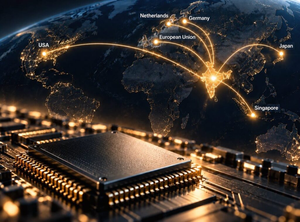
The international dimension of India’s semiconductor strategy was particularly visible through dedicated country roundtables. The India-USA Semiconductor and Electronics Ecosystem Roundtable brought together representatives from 64 Indian companies and 52 international organisations. Discussions covered commercial partnerships, joint ventures, research and development, supply chains and workforce skills.
The India-Japan Semiconductor Roundtable focused on combining Japanese strengths in equipment, materials and precision manufacturing with India’s design talent, domestic demand and expanding production base.
Participants discussed joint ventures, technology transfers, local supply chains and research cooperation. These relationships reflect the international nature of semiconductor manufacturing, where no single country typically controls every stage of the value chain.
India is also attempting to strengthen the link between semiconductor manufacturing and the next generation of chip designers.
PM Modi met 20 students from academic institutions across the country who presented 20 chips that they had designed, fabricated and tested for different applications. The event’s Startup Pavilion, Student Hackathon, Innovation Showcase and Workforce Development Pavilion further connect industry with universities and emerging companies.
WATCH ALSO: https://modernmechanics24.com/post/lockheed-martin-grizzlymissile-launcher/
The global market provides a substantial backdrop to these efforts. SEMI President and CEO Ajit Manocha said the semiconductor industry could reach USD 3 trillion by 2035 and called for India to develop capabilities across critical parts of the value chain. That includes not only factories but also equipment, materials, design, packaging, research and specialist skills.
The scale of SEMICON India reflects this international focus. The 2026 event features representatives from 52 countries, more than 400 executives and over 150 speakers, with country pavilions from Japan, South Korea, Malaysia, the Netherlands, Singapore and Sweden. Organisers expect about 50,000 visitors during the three-day exhibition.
India’s semiconductor strategy is, therefore, entering a more demanding stage. The initial challenge was establishing policy support and attracting major projects, while the next challenge is making factories operational and connecting them to reliable domestic and international suppliers.
Semicon 2.0 places that broader ecosystem at the centre of the strategy, with the coming years set to show how effectively India’s investments in fabs, packaging, design, research and talent translate into sustained semiconductor production.









One Response