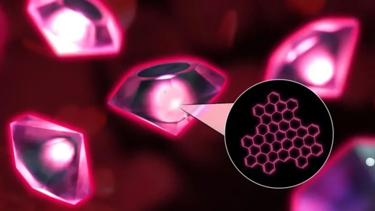

Researchers at ETH Zurich have developed a new type of pixel that can both display and analyze light.
The innovation combines functions that have traditionally required separate technologies, such as screens and camera sensors. The advance opens new possibilities for future devices that can capture, process, and display visual information within the same system.
For nearly a century, pixels have served one of two purposes. They either create images on displays or capture images inside cameras. Until now, no single pixel has been able to perform both tasks.
A research team led by Professor David Norris at ETH Zurich has changed that. The scientists developed a bidirectional pixel. These pixels can control and analyze light simultaneously.
The study was recently published in the scientific journal Nature. The research represents a new approach to managing light within optical devices. It also lays the foundation for future systems that combine imaging and display technologies.
The concept builds on a fundamental property of light known as interference. This effect occurs when multiple light waves overlap. Depending on how those waves align, they either reinforce each other or cancel each other out.
READ ALSO: Lost for 80 Years: Hiroshima Survivor’s Memoir Found and Set for Global Release
Scientists have studied interference for many years. It plays an important role in optics, imaging, and communication technologies. The ETH Zurich team used this principle to create a highly versatile pixel.
Their work relies on specially engineered surfaces. These surfaces are sculpted with extreme precision at the nanometer scale. A nanometer is one billionth of a meter.
The researchers developed a process that shapes these surfaces with remarkable accuracy. The tiny structures guide light in very specific ways. This allows the pixel to perform functions that conventional pixels cannot.
How ETH’s Fourier Pixel Controls
The new technology is based on a Fourier pixel, as the researchers call it. The name comes from Fourier analysis, a mathematical method used to understand complex wave patterns. This technique helps scientists predict how light behaves after interacting with the pixel.
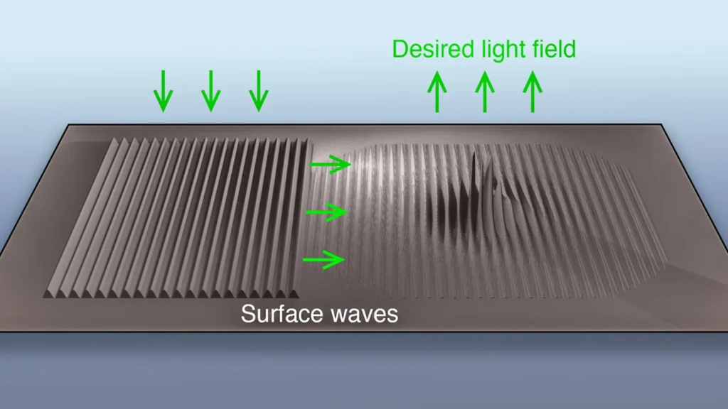
Inside the pixel, incoming light is first converted into a surface wave. These waves travel through the material rather than moving freely through space. Scientists refer to them as surface plasmon polaritons.
As the wave moves across the pixel, it encounters carefully designed surface structures. These structures scatter the wave back into light. The resulting light waves then interfere with one another.
This interference creates specific images and patterns. By changing the surface design, researchers can control the final result. The process gives them precise control over how light behaves.
The technology does more than manage brightness. It also controls important properties of light such as phase and polarization. These characteristics are essential in many advanced optical systems.
Polarization describes the direction in which a light wave vibrates. Different polarization states are used in imaging, sensing, and communication technologies. The ETH Zurich team can generate and manipulate these states directly within the pixel.
Doctoral researcher Yannik Glauser explained that the system controls polarization by combining surface waves with different orientations. The final polarization depends on the shape of the pixel’s surface. This provides a high level of control over the outgoing light.
The researchers can also manipulate the phase of light. Phase describes the position of a light wave within its oscillation cycle. Controlling phase enables the creation of unique beam shapes.
One example is a doughnut-shaped light beam. These beams contain a dark central region surrounded by light. They are useful in several scientific and technological applications.
The technology also works with multiple wavelengths of light. This means it can create colored images rather than being limited to a single color. Such flexibility expands the range of possible applications.
READ ALSO: Arizona Scientists Uncover the Wanderlust of America’s Iconic Bald Eagles
Camera and Display Functions in One Device
The same principles that allow the pixel to control light also allow it to analyze light. This dual functionality makes the technology especially significant. Traditional displays and cameras require separate components.
To analyze light, the researchers reverse the process. They combine incoming light with a reference wave on the pixel. This interaction creates an interference pattern.
A camera captures the resulting pattern. Using mathematical analysis, researchers can determine the phase of the incoming light. The same approach can also reveal its polarization state.
Postdoctoral researcher Sander Vonk said the Fourier-based design allows multiple functions to be combined within a single pixel. The method simplifies the design process because Fourier analysis is mathematically straightforward. It also reduces the need for highly complex computational models.
The implications extend far beyond displays and cameras. Light-based technologies are found in smartphones, televisions, optical sensors, medical instruments, and fiber-optic communication networks. Improvements in light control can therefore affect many industries.
The researchers also see potential for direct optical computing. Since surface waves can perform mathematical operations within the material itself, future devices could process visual information without sending data to a separate computer processor. This could improve efficiency and reduce system complexity.
WATCH ALSO: World’s first motorbike backflip between two moving trucks successfully completed
A key next step is scaling the technology into larger arrays. Modern displays and image sensors contain millions of pixels working together. The researchers aim to create matrices made up of many Fourier pixels that can operate as integrated camera-display systems.
The innovation has already moved beyond the laboratory stage. The research team has filed a patent application related to the technology. The invention has also been nominated for this year’s Spark Award.
However, bidirectional pixels could reshape the design of future optical devices. By combining light generation and analysis within a single tiny component, the technology points toward a future in which displays, cameras, and optical processors are more closely integrated than ever before.