A new method developed by researchers in South Korea and the US has improved the efficiency and durability of perovskite solar cells.
The team discovered that direct contact between 2D and 3D perovskite materials can reorganize crystal structures inside solar films.
Their approach helped solar cells achieve 26.25% efficiency while also improving long-term operational stability.
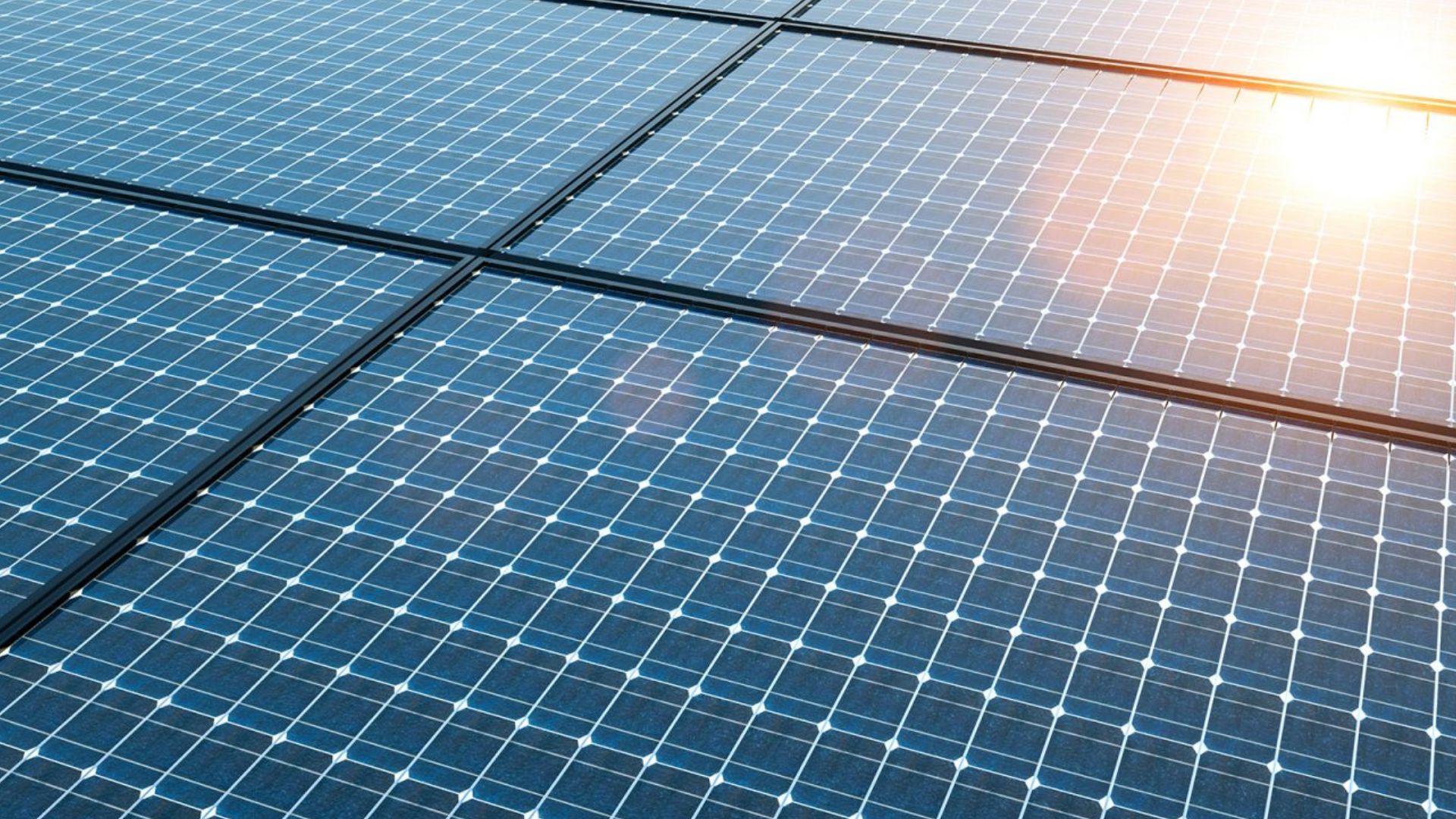
Perovskite solar cells have attracted global attention because they are cheaper and easier to produce than traditional silicon solar panels. These materials can convert sunlight into electricity with very high efficiency while remaining lightweight and flexible. Scientists believe they could play a major role in the future of clean energy technologies.
One of the biggest challenges facing perovskite solar cells is stability. Many perovskite materials degrade over time because their crystal structures contain defects and structural weaknesses. These imperfections reduce energy conversion efficiency and shorten device lifespan.
READ ALSO: African Lion 26 Tests US Army Robotic Ground Vehicles in Counterattack Drill in Morocco
Researchers from Korea University, the University of Toledo, and Seoul National University developed a new process to solve this issue. Their findings were published in the scientific journal Nature Energy.
The study focused on improving the internal crystal order of FAPbI₃ perovskite films, one of the most important materials used in high-efficiency solar cells.
2D and 3D Perovskites Improve Crystal Quality
The researchers explored interactions between two-dimensional and three-dimensional halide perovskites.
In simple terms, 2D perovskites are thinner-layered materials, while 3D perovskites have a bulk crystal structure that absorbs sunlight more efficiently. Combining the two allows scientists to improve the stability of solar cell surfaces and interfaces.
Jun Hong Noh, one of the senior researchers involved in the project, explained that scientists have long believed similar materials on both sides of a light-absorbing layer can improve solar cell performance. This idea is already used in advanced silicon and gallium arsenide solar technologies.
However, applying the same concept to halide perovskites has been difficult because these materials behave differently during manufacturing.
To address this problem, the team used wide-bandgap 2D halide perovskites. Wide-bandgap materials absorb higher-energy light, such as blue and ultraviolet wavelengths. They also help stabilize neighboring layers by reducing unwanted energy losses.
The researchers had already developed a method in 2021 to create a 2D and 3D perovskite junction without causing damaging chemical reactions between the layers. Their technique involved placing a 2D film directly on top of a 3D film while applying heat and pressure. This process produced highly ordered crystal layers with fewer defects.
WATCH ALSO: India recently tested carried out the successful launch of Intermediate Range Agni-Prime Missile
During their latest experiments, the researchers made an unexpected discovery. They found that simply bringing the 2D and 3D materials into contact altered the optical properties of the 3D layer. This happened even before heat or pressure was applied.
The team observed changes in photoluminescence, which is the light emitted by a material after it absorbs energy. These changes depended strongly on the organic molecules inside the 2D layer. Researchers said the interactions between the organic cations in both materials played a major role in reorganizing the crystal structure.
New Contact Method Raises Solar Cell Efficiency
The researchers then added a thermal treatment step after the two layers were brought together. They believed that heating the materials while they were already interacting would create a stronger, more stable crystal structure. Their results confirmed this idea.
The process improved pristine FAPbI₃ films without the use of chemical additives. Many earlier studies relied on additives to improve crystal growth, but additives can sometimes create long-term stability concerns. The new method avoided that problem entirely.
The refined films showed crystal structures very close to their ideal theoretical arrangement. This is important because defects within perovskite crystals act as traps, wasting electrical energy. Fewer defects mean more electricity can be produced from sunlight.
The researchers also found that the films resisted unwanted phase transitions. Perovskite materials often transform into less useful crystal forms over time, especially under heat or moisture. The improved films maintained their desirable structure much longer than standard versions.
To test real-world performance, the team integrated the films into working solar cells. The devices achieved certified power conversion efficiencies of 26.25%. That level places them among the highest-performing perovskite solar cells reported so far.
The solar cells also demonstrated strong operational durability. Under accelerated testing conditions, they maintained performance for roughly 24,000 hours. Long operational life is considered essential before perovskite technology can be widely commercialized.
Why the Discovery Matters for Future Solar Technology
The findings arrive at an important time for the global solar industry. Governments and energy companies are seeking cheaper, more efficient alternatives to silicon solar panels. Perovskite materials are considered among the strongest candidates because they can be manufactured at lower temperatures and lower cost.
Another advantage of the new method is scalability. The contact-based process can potentially be applied to larger solar films without introducing many defects. This could help manufacturers produce large-area perovskite panels more consistently in commercial factories.
The approach may also support the development of tandem solar cells. Tandem devices combine multiple light-absorbing materials to capture a wider range of sunlight. Many next-generation solar technologies rely on tandem structures to push efficiencies beyond the limits of conventional silicon panels.
Researchers said the method may be especially useful for low-temperature processing systems. Some tandem solar cells require delicate layers that cannot tolerate high heat during production. The new contact-induced crystallization strategy may allow high-quality crystal growth even under those restricted conditions.
READ ALSO: Biogas Output Soars 200% as Wastewater System Converts Sewage Sludge to Renewable Gas
Scientists now plan to study whether even more structurally perfect 2D and 3D materials can further strengthen the observed effects. Better crystal quality in both layers may improve performance and reveal additional physical properties. The team believes their discovery opens a new pathway for designing stable and efficient perovskite devices.
Perovskite solar technology has advanced rapidly over the past decade, but stability concerns have slowed commercial deployment. This new study addresses one of the field’s most critical problems by improving crystal order without the use of additives.
If successfully scaled for industrial production, the method may help accelerate the arrival of cheaper, high-efficiency solar panels for homes, vehicles, and future energy systems.