
Researchers from the National University of Singapore (NUS) and Applied Materials have developed an atom-thin coating that addresses one of the biggest challenges facing future semiconductor chip wiring.
The new material replaces thicker protective layers used in copper wiring and allows more space for electrical current to flow. The innovation supports continued chip miniaturization while improving performance, efficiency, and reliability.
Atom-Thin Coating Targets Chip Wiring Bottleneck
The global semiconductor industry is moving toward annual sales of nearly $1 trillion. Demand continues to grow as artificial intelligence, high-performance computing, smartphones, and advanced electronics require more powerful chips.
For decades, chipmakers improved performance by making transistors smaller. This approach allowed more transistors to fit onto a chip and increased computing power.
However, shrinking transistors is no longer the only challenge. Another major obstacle is emerging within the tiny wiring network that connects billions of transistors.
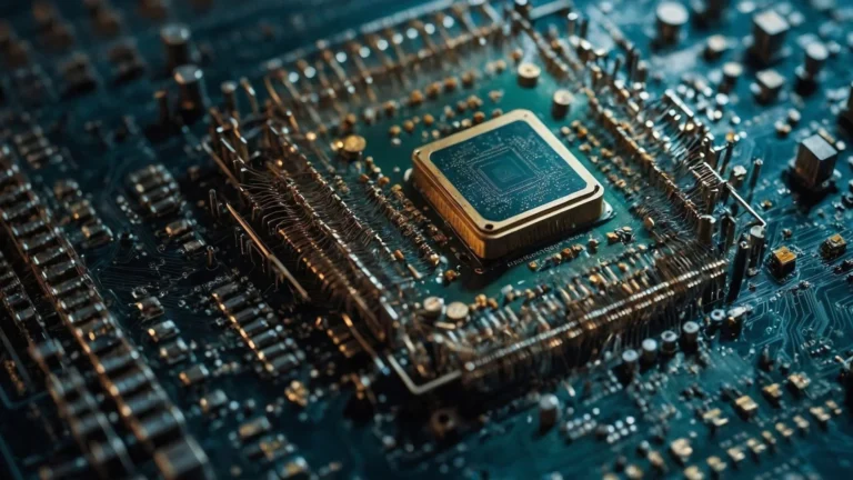
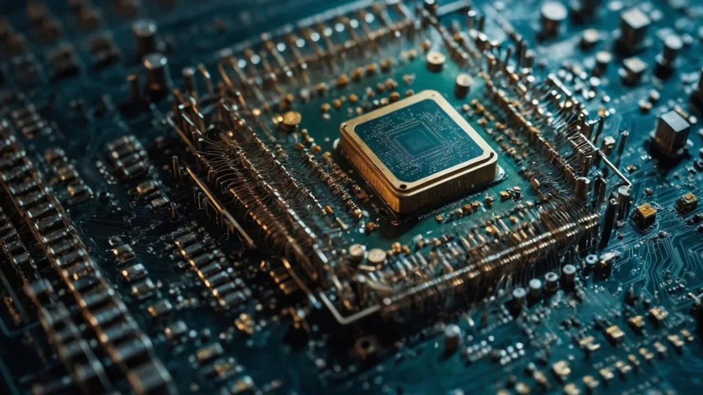
These microscopic wires are typically made of copper. They carry electrical signals across the chip and play a critical role in overall performance.
Copper wiring requires protective coatings to function properly. One coating acts as a barrier, preventing copper atoms from leaking into surrounding materials, while another serves as a liner, helping copper adhere to surfaces and form reliable connections.
Current semiconductor manufacturing relies on tantalum-based materials for these functions. These coatings generally need a thickness of at least four nanometers to work effectively.
READ ALSO: Compact Imaging Chip Sees Beyond Color, Revealing What Cameras Always Missed
As chips continue to shrink, these protective layers occupy an increasing share of available space. This leaves less room for copper, increasing electrical resistance and reducing performance.
Researchers from NUS and Applied Materials have now developed a single material that performs both protective functions. The material is tungsten disulfide, commonly known as WS2.
The team successfully grew crystalline WS2 films measuring only 0.7 nanometers thick. That thickness is roughly equivalent to a few atoms stacked on top of each other.
The films were produced on industry-standard 200-millimeter semiconductor wafers. Their findings were published in the scientific journal Nature Electronics.
WS2 Replaces Two Layers With One
The research showed that a single atomic layer of WS2 can act as both a liner and a barrier. This eliminates the need for separate protective materials around copper wiring.
One of the first tests focused on the linear function. Researchers examined how copper behaved when deposited onto chip surfaces.
Without a liner, ultrathin copper tends to form isolated clusters instead of a smooth film. These clusters create poor electrical pathways, increasing resistance.
The WS2 coating helped copper spread evenly across the surface. As a result, electrical resistance dropped by more than a million times compared with uncoated surfaces.
The researchers also compared the new coating with conventional tantalum-based materials. Despite being nearly ten times thinner, the WS2 layer delivered about five times better performance.
The difference becomes especially important as wiring dimensions continue to shrink. In a future copper wire measuring 20 nanometers in diameter, traditional protective coatings would consume about 40% of the wire’s diameter.
The WS2 coating occupies only about 7% of that space. This leaves much more room for copper to carry electrical current. More copper inside each wire means lower resistance. Lower resistance improves speed and reduces energy losses within the chip.
READ ALSO: China’s Origin Wukong Quantum Computer Tops One Million Tasks With Built-In Security
Chip Wiring, Reimagined Thin
The researchers then tested the barrier capabilities of the atom-thin layer. They wanted to determine whether such a thin material could effectively block copper migration.
Heat stress tests revealed clear differences between protected and unprotected surfaces. Copper on uncoated silicon reacted with the underlying materials, creating large defects.
The WS2-coated samples showed no signs of reaction or intermixing. The protective layer successfully prevented copper atoms from penetrating surrounding materials.
Additional electrical stress testing produced similar results. The WS2 barrier increased projected wire lifetimes by more than ten times compared with unprotected structures.
Dr. M. Juvaid Mangattuchali, who co-led the research, said the process works across full semiconductor wafers and operates at relatively low temperatures. This makes it compatible with the semiconductor industry’s existing manufacturing processes.
Professor Silvija Gradečak from NUS explained that the key achievement was proving that a single atomic layer can replace the conventional two-layer system. This creates a new approach for designing future chip interconnects.
Industry-Compatible Process Supports Future Chips
Developing a high-performance material is only part of the challenge. Semiconductor manufacturers also need processes that fit into existing production lines.
The research team addressed this requirement by using thermal atomic layer deposition. The process operates at 350 degrees Celsius without plasma treatment.
This manufacturing approach satisfies several important industry requirements. First, the temperature is low enough to prevent damage to the delicate layers already present on semiconductor wafers.
Second, the process provides a uniform coating across an entire wafer. Uniformity is essential for producing reliable chips at scale.
Third, engineers can precisely control thickness down to a single atomic layer. Such accuracy becomes increasingly important as chip features continue to shrink.
Fourth, the coating can cover deep, narrow trenches found in advanced semiconductor designs. The team achieved more than 95% coverage in structures with a depth-to-width ratio of 10:1.
Researchers also used computational modeling to understand why WS2 performs so well as a barrier material. The simulations were carried out by scientists from the NUS Department of Chemistry.
WATCH ALSO: SpaceX is gearing up to conduct 11th flight test of Starship on October 13
The WS2 films contain numerous tiny crystalline grains. Unlike a perfect crystal, these grains point in different directions throughout the material.
This structure creates a complex path for copper atoms attempting to move through the layer. Researchers compared the arrangement to offset joints in a brick wall.
Because defects do not line up across multiple layers, copper atoms face a much more difficult route. This greatly reduces the chance of unwanted diffusion.
Professor Richard Wong explained that the polycrystalline structure turned out to be an advantage rather than a weakness. The grain arrangement naturally strengthens the barrier performance.
According to the research team, the achieved thickness is below the target for any barrier or liner listed in international semiconductor technology roadmaps through 2037. This positions the technology for multiple future generations of advanced chips.
The development is especially significant for semiconductor-producing nations such as Singapore, which manufactures about 1 in 10 chips globally. Improvements in wiring technology can help sustain progress as traditional transistor scaling becomes more difficult.
Researchers plan to continue studying the microscopic interface between copper and WS2. They also aim to explore whether greater control over grain orientation can further improve reliability and performance.
The work demonstrates that atomically thin two-dimensional materials can be integrated into commercial semiconductor manufacturing.