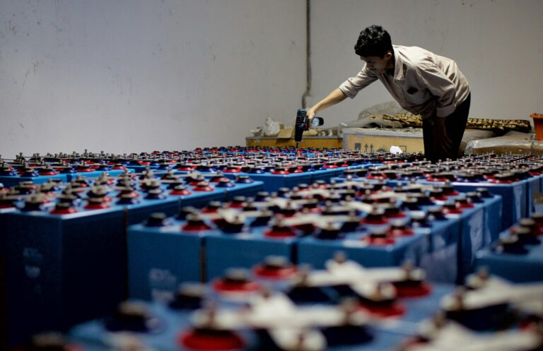

As silicon-based chips inch closer to their physical limits, Chinese scientists unveiled a new technique to mass-produce large, high-quality two-dimensional (2D) semiconductor wafers.
This development could accelerate the transition beyond conventional silicon technology, marking a step towards the next era of electronics.
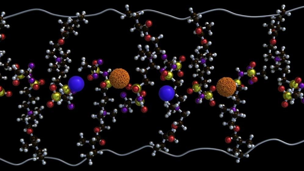
The finding is based on molybdenum disulfide (MoS₂). It is an atomically thin material widely viewed as one of the strongest candidates for post-Moore’s Law semiconductor devices. MoS₂ has high carrier mobility and low power consumption. Producing large, uniform, defect-free wafers is suitable for industrial-scale manufacturing.
A research team led by Wang Jinlan of Southeast University in Nanjing, and Wang Xinran and Li Taotao from Nanjing University successfully fabricated a 6-inch (150mm) single-crystalline MoS₂ wafer. The study was published in the peer-reviewed journal Science on January 29.
“For 2D semiconductors to move from laboratory curiosity to industrial reality, large-area uniform growth is essential,” the researchers wrote.
READ ALSO: https://modernmechanics24.com/post/china-overtakes-us-in-hypersonic-arms/
MoS₂ crystals are grown using chemical vapor deposition (CVD), where gaseous precursors form thin films on substrates. While CVD produces high-quality samples, it struggles to scale up beyond small laboratory sizes.
Metal-organic chemical vapor deposition (MOCVD) has enabled scalability, with films as large as 8 inches.
However, MOCVD brings new challenges. Metal-organic precursors often leave carbon impurities in the crystal lattice, degrading performance. In addition, crystal growth rates remain slow, and defects accumulate across larger surfaces.
Wang’s team identified a bottleneck in the crystallization process that required significant energy input, limiting both speed and quality. Instead of pushing through this energy barrier, the researchers found a way around it.
By introducing oxygen into the reaction process, they created an alternative growth pathway that reduced the energy requirement. The team named the method oxy-MOCVD.
Using a sapphire substrate, the researchers grew a uniform 6-inch single-crystalline MoS₂ film. The results were striking. The growth rate exceeded conventional MOCVD by more than two orders of magnitude while eliminating carbon contamination.
“This approach bridges the gap between lab-scale CVD quality and industrial-scale MOCVD scalability,” the researchers said.
WATCH ALSO: https://modernmechanics24.com/post/drdo-akhash-ng-missile-trials-success/
To test the material’s electronic performance, the team fabricated field-effect transistor (FET) arrays from the 6-inch wafer. The devices demonstrated electron mobility more than 10 times higher than that of transistors made using traditional MOCVD-grown MoS₂.
Higher mobility translates to faster switching speeds and lower power consumption. These are key attributes for next-generation processors, artificial intelligence hardware, and energy-efficient electronics.
The development comes as semiconductor engineers worldwide search for alternatives to silicon. As transistor sizes shrink toward atomic scales, further miniaturization of silicon becomes increasingly difficult and expensive. Atomically thin 2D materials offer a potential solution by enabling ultra-thin channels without sacrificing electrical performance.
A week after the oxy-MOCVD study appeared in Science, researchers at the University of Science and Technology, Beijing, reported a technique that allows real-time observation of MoS₂ crystal growth under a transmission electron microscope (TEM). This capability could further reduce surface defects and refine growth precision.
Chinese research teams have been working on advancing 2D semiconductor technology in recent years. In 2023, a group led by Liu Kaihui at Peking University demonstrated the batch production of MoS₂ wafers ranging from 2 to 12 inches in diameter using a substrate-stacking method. The same team later proposed a strategy for producing 2-inch single-phase indium selenide (In₂Se₃) wafers.
READ ALSO: https://modernmechanics24.com/post/titanic-sized-electric-ferry-set-record/
Meanwhile, researchers at Fudan University in Shanghai developed the world’s first 32-bit RISC-V microprocessor built entirely from 2D semiconductor materials. The processor is named Wuji. It operates using 5,900 MoS₂ transistors and executes standard 32-bit instructions.
Silicon will not disappear overnight. But 2D materials are strong contenders for future chip architectures, particularly in ultra-low-power and flexible electronics. The successful fabrication of a 6-inch single-crystalline MoS₂ wafer marked a pivotal moment in that journey.