

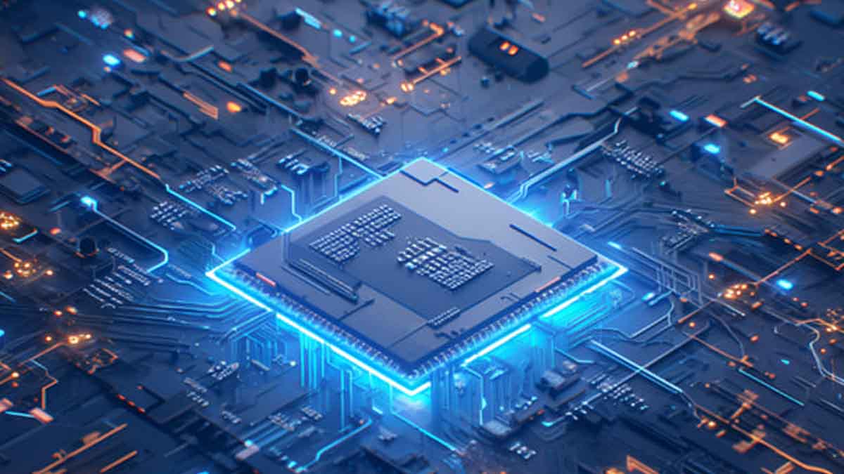
Huawei Technologies has released a new research paper detailing how its Tau Scaling Law semiconductor architecture manages heat in advanced smartphone processors.
The study was published on Friday on ChinaXiv, a scientific publication platform for papers that have not yet undergone peer review.
The paper was authored by He Tingbo, chairwoman of Huawei’s Scientist Committee and president of the company’s semiconductor business department. It focuses on thermal performance, which many analysts viewed as one of the biggest challenges facing Huawei’s next-generation chip strategy.
According to the paper, measurements from the upcoming Kirin 2026 processor show lower operating temperatures than its predecessor. This was achieved despite increasing transistor density by 55 percent per square millimetre.
Huawei said the chip also reduced power consumption significantly during several key computing tasks. In some workloads, energy use fell by as much as 66 percent compared with earlier designs.
READ ALSO: https://modernmechanics24.com/post/us-gps-free-aircraft-navigation-pacific/
Inside Tau Architecture
Tau Scaling Law is Huawei’s proposed path for advancing semiconductor performance without relying on the most advanced extreme ultraviolet lithography equipment. Such machines remain unavailable to Chinese companies due to export restrictions imposed by the US.
The framework relies on a technology called LogicFolding, which vertically stacks active chip layers. Instead of spreading components across a larger surface area, the design places them closer together in multiple tiers.
Huawei said this arrangement shortens the distance that electronic signals travel between different processing units. Shorter pathways reduce energy loss and improve efficiency across critical components such as central processing units, graphics processors, neural processing units and digital signal processors.
These components generate a large share of the heat inside modern smartphone chips. By reducing unnecessary energy consumption, Huawei said the new design lowers overall thermal output while increasing computing capability.
The paper directly challenges concerns that stacking active layers would automatically create overheating problems. He wrote that testing results from the new Kirin processor contradicted those assumptions.
Efficiency Through Design
Analysts said Huawei addressed thermal management through a combination of architectural and physical design changes. The company reduced source power density by folding chip structures in ways that prevent excessive heat from building up in specific locations.
Engineers also paid close attention to thermal placement during the design stage. The most heat-intensive modules were positioned where heat could move away more efficiently.
In a research note released on Saturday, Kaiyuan Securities said the architecture successfully balances performance and power efficiency. The brokerage noted that the chip can adapt between power-saving requirements and maximum performance demands.
According to Kaiyuan analysts, the combination of lower power consumption and higher transistor density gives Huawei greater flexibility when managing performance under different operating conditions. This helps maintain stable operation while avoiding excessive temperatures.
WATCH ALSO: https://modernmechanics24.com/post/china-trains-hq17-type-625-air-defense/
Industry Watches Closely
Huawei first introduced its Tau Scaling Law concept in May. At the time, the company claimed the architecture could eventually deliver transistor densities comparable to leading-edge 1.4-nanometre manufacturing processes by 2031.
A second paper published in July reported that the Kirin 2026 processor remained on track for a 55 percent density improvement over the Kirin 9030 Pro. The latest study adds thermal performance data to support those earlier projections.
Zheng Lei, chief economist at Samoyed Cloud Technology Group, described the approach as a practical response to Huawei’s long-term performance goals. He said the method still has limitations but offers room for further development and refinement.
Industry observers believe Huawei’s work may influence a wider group of Chinese semiconductor companies. Areas such as chip manufacturing, advanced packaging, testing technologies and semiconductor equipment may benefit from innovations linked to thermal management.
Zhang Xinyuan, an analyst at Beijing-based think tank Kefangde, said the approach could also encourage research into new semiconductor materials and advanced 3D integration technologies. These technologies are becoming increasingly important as chipmakers seek ways to improve performance beyond traditional scaling methods.
Huawei’s latest findings arrive as the global semiconductor industry searches for alternatives to conventional chip miniaturisation. If the company’s thermal management approach performs as expected in commercial devices, it may play an important role in shaping the next generation of smartphone processor design.
READ ALSO: https://modernmechanics24.com/post/new-chip-withstands600c-venus-missions/
A useful follow-up angle would be comparing Huawei’s Tau Scaling Law with Intel, TSMC and Samsung’s 3D chip-stacking strategies to assess how the approaches differ in performance and manufacturing requirements.






One Response