Researchers at the Massachusetts Institute of Technology (MIT) have reported major progress in developing advanced chip technology that combines electronics and photonics to deliver significantly faster and more energy-efficient data communication.
The work is part of the FUTUR-IC research program, launched in 2022 to develop future semiconductor systems that can handle growing data demands while reducing energy consumption. The project also focuses on making these advanced chips easier and less expensive to manufacture using existing semiconductor production infrastructure.
Faster Data Transfer
The FUTUR-IC program integrates electronics, which process information using electrical signals, with photonics, which transmit information using light.
This combination allows data to move much faster while consuming less power than conventional electronic-only systems. Researchers say the technology aims to increase communication speeds from today’s hundreds of terabits per second to more than one petabit per second.
Program leader Anu Agarwal said the integrated systems are designed to provide greater bandwidth while improving energy efficiency. She explained that combining electronics for computing with photonics for communication helps address the increasing power demands of modern data processing. The concept also supports more sustainable computing as global digital infrastructure continues to expand.
Current systems mainly rely on electronics or pluggable optical connections for data transfer between chips. The new approach uses co-packaged optics, in which electronic and photonic components are integrated into a single package. This design shortens communication distances, improves performance, and reduces energy losses during data transmission.
Chip Technology Speeds Data
One of the biggest challenges in combining electronics and photonics has been efficiently connecting the two technologies. Existing methods remain expensive because the manufacturing ecosystem for co-packaged optics is still developing. FUTUR-IC researchers addressed this issue by creating new optical connection devices that simplify integration.
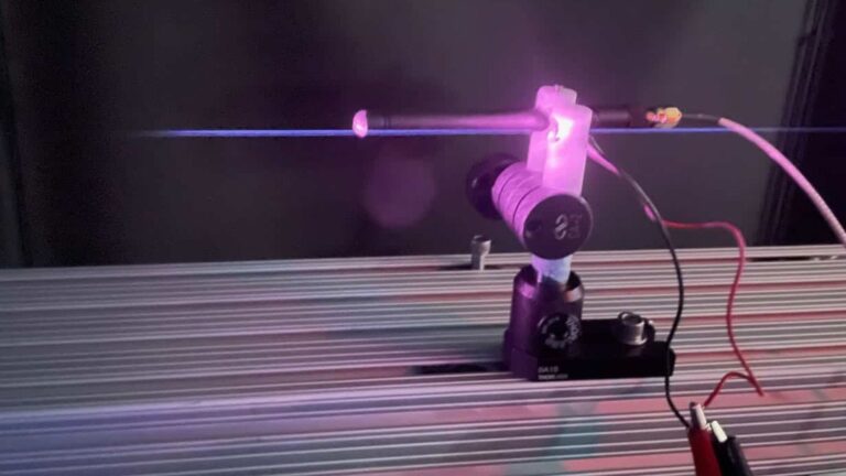
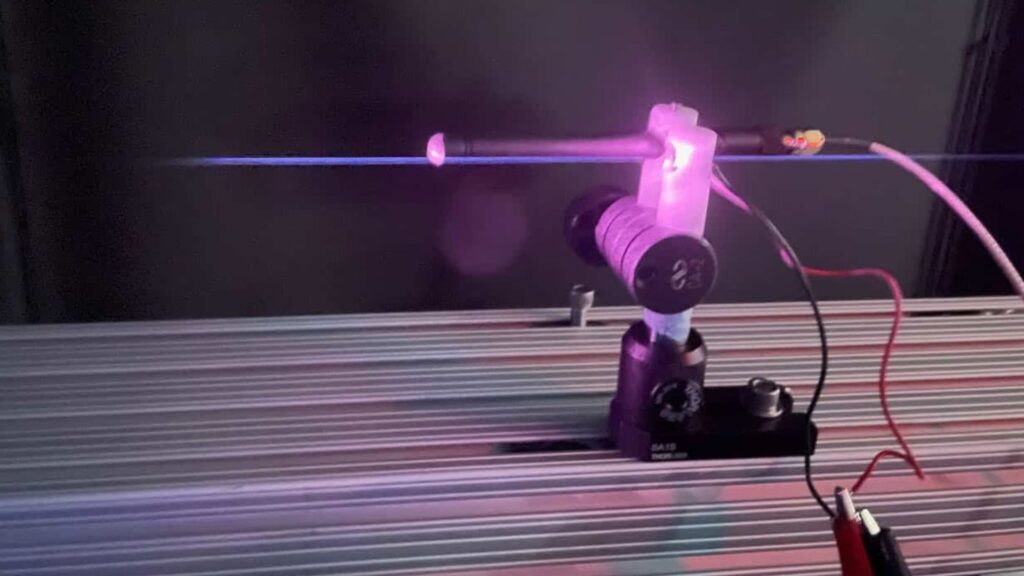
The team developed two optical couplers known as the evanescent coupler and the graded-index (GRIN) coupler. The evanescent coupler appeared on the cover of Advanced Engineering Materials last year, while the GRIN coupler was detailed in the March 2026 issue of the Journal of Physics: Photonics. A third optical coupler, developed by an MIT team led by Professor Juejun Hu, was published earlier in Laser & Photonics Reviews with support from the US Department of Energy.
Researchers describe these devices as the optical equivalent of solder bumps used in electronic chips. Traditional solder bumps create electrical connections between chips, while the new optical bumps allow light signals to move between photonic components. Until these developments, no comparable optical connectors existed for chip packaging.
Drew Weninger, first author of the studies on the evanescent and GRIN couplers, explained that future photonic chips will require both electrical and optical connections. He said different optical bump designs offer different advantages depending on the application. The GRIN coupler supports a wider range of light wavelengths, while the evanescent coupler is easier to manufacture and allows denser chip connections.
Addressing Energy Challenges
The research also addresses growing environmental concerns associated with the semiconductor industry. Microchips used in consumer electronics, communication systems, and medical equipment generated an estimated 500 megatons of carbon dioxide-equivalent emissions during their lifetime in 2021. At the same time, the world produces more than 50 million tons of electronic waste every year.
Demand for computing power continues to grow due to cloud services, artificial intelligence, and video streaming. Researchers estimate that data centers may consume nearly 10 percent of global electricity by 2030 if current trends continue. Improving communication efficiency inside computing systems has therefore become an important priority for both industry and researchers.
READ ALSO: US Navy Advances Trident II D5LE2 and W93 Warhead to Strengthen Nuclear Deterrence
Agarwal said transmitting information with light requires much less energy than moving it with electrical signals alone. By assigning computing tasks to electronics and communication tasks to photonics, the project seeks to reduce the overall power required by future computing systems. This approach also supports long-term efforts to make digital infrastructure more sustainable.
Building Future Ecosystem
FUTUR-IC extends beyond hardware development and includes work on sustainability tools and workforce training. One initiative, called Earthster, helps companies evaluate the environmental impact of their products by mapping energy use, material consumption, and carbon emissions across supply chains. The platform enables manufacturers to identify areas where emissions can be reduced more effectively.
The program also supports education through online courses, hands-on training, and digital learning platforms focused on semiconductor resource efficiency. Summer academies, boot camps, and interactive learning activities help prepare students and professionals for future semiconductor technologies. For younger learners, FUTUR-IC has produced educational TED-Ed videos that introduce semiconductor concepts in an accessible format.
The GRIN coupler research involved additional contributions from Lionel Kimerling, Christian Duessel, Samuel Serna, and other collaborators from MIT and Bridgewater State University. Researchers also published a review in Nature that describes the growing range of optical coupler technologies and explains why multiple connector designs will be needed for different applications.
As the semiconductor industry seeks faster, more efficient computing systems, the advances made through FUTUR-IC are expected to support future chip packaging, data centers, communications infrastructure, and next-generation computing technologies.