
Scientists at the National Institute of Standards and Technology (NIST) have developed a new packaging method for photonic integrated circuits that enables them to survive and function in extreme environments.
These tiny chips use light rather than electricity to carry information, making them much faster and more energy-efficient than traditional electronic chips.
Despite their advantages, their real-world use has remained limited because their packaging cannot withstand harsh conditions.
The new method aims to change that limitation. With this advancement, photonic chips can now be used in demanding environments, including deep-space missions, nuclear reactors, ultrahigh-vacuum systems, and extreme-temperature environments ranging from near absolute zero to intense industrial heat. These are places where conventional semiconductor chips often fail or lose efficiency.
READ ALSO: Rostov Reactor Test Concludes: Russia Pushes New Era of Nuclear Fuel Design
Photonic chips already play an important role in telecommunications, medical diagnostics, and advanced sensing technologies.
However, expanding their use into more extreme and high-risk environments has always been a challenge. The new packaging approach developed by NIST opens the door for wider applications across industries that demand both performance and durability.
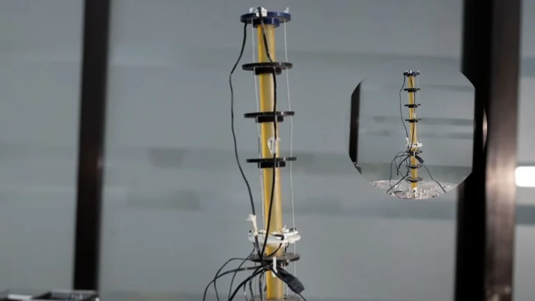
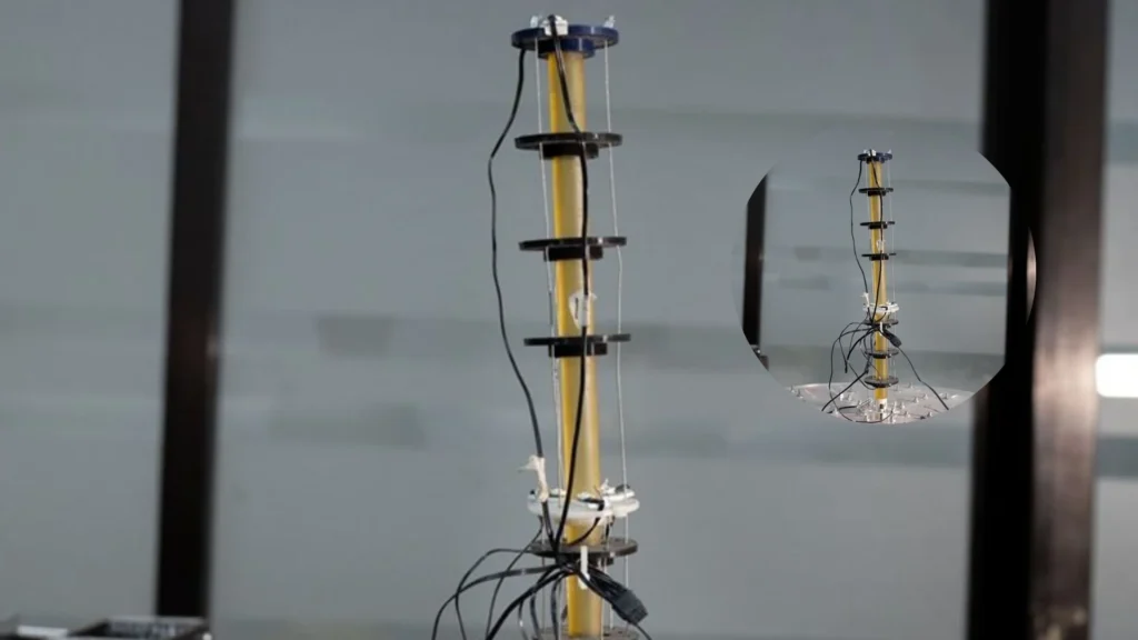
Photonic Chips: From Fragile Connections to Strong Bonds
In the world of microelectronics, packaging is not just a protective outer layer. It is a key system that connects the chip to optical fibers, electrical contacts, and other components.
For photonic chips, maintaining perfect alignment between the chip and the optical fiber is essential. Even the smallest misalignment can interrupt the flow of light and cause the system to fail.
Until now, most packaging methods have relied on organic adhesives. These materials, similar to specialized glues, are not suitable for extreme environments.
WATCH ALSO: China commissions world’s largest open-sea offshore solar photovoltaic project
They can crack under very low temperatures, degrade when exposed to radiation, and release gases in vacuum conditions. Over time, these effects weaken the bond, making the chip unreliable or completely unusable.
To overcome this issue, NIST researchers turned to a technique originally developed by NASA known as Hydroxide Catalysis Bonding (HCB). Instead of using glue, this method uses a small amount of sodium hydroxide solution to chemically bond the optical fiber to the photonic chip.
The process creates a glass-like molecular-level connection, forming a rigid, stable link between the two components. This approach not only improves durability but also ensures precise alignment, which is essential for photonic systems.
Lead researcher Nikolai Klimov highlighted the importance of this development. He said the study marks a major step toward bringing the speed and efficiency of photonics into environments where traditional chips cannot operate.
Tested in Extreme Conditions, Ready for the Future
The NIST team carried out a series of rigorous tests to evaluate the strength and reliability of the new packaging method.
The packaged photonic chips were exposed to cryogenic temperatures, rapid temperature fluctuations, high vacuum conditions, and intense ionizing radiation. These tests were designed to simulate the harsh environments found in space missions, quantum computing systems, and nuclear facilities.
READ ALSO: After 81 Years, Volkswagen WWII Past Meets Israel Rafael Deal Beyond Cars and Crisis
Even after undergoing these extreme conditions, the bond between the optical fiber and the chip remained intact. More importantly, the photonic chip continued to function normally, proving the effectiveness of the new packaging technique. This level of resilience is a significant improvement over traditional adhesive-based methods.
High-temperature testing of the fully packaged chip was limited. This was due to the limitations of currently available optical fibers.
However, additional studies were done separately. These showed that the HCB method remains stable even at much higher temperatures than those of regular adhesives. This means the technique can work well in high-temperature industrial environments.
At present, the bonding process takes several days to complete. However, researchers emphasize that this is not a fundamental limitation. With further engineering and optimization, the process time can be reduced significantly, making it suitable for large-scale manufacturing.
WATCH ALSO: Chinese humanoid robot plays basketball with almost human-like accuracy
Klimov stated that the bond created through this method is as resilient as the optical fiber itself. This strength enables photonic chips to operate in environments previously out of reach. The development is expected to benefit a wide range of fields, including quantum computing, space exploration, particle physics, and industrial sensing.
As industries continue to push technological boundaries, the need for reliable systems in extreme conditions is growing. This new packaging method represents an important step forward, bringing photonic technology closer to widespread use in some of the most challenging environments known.