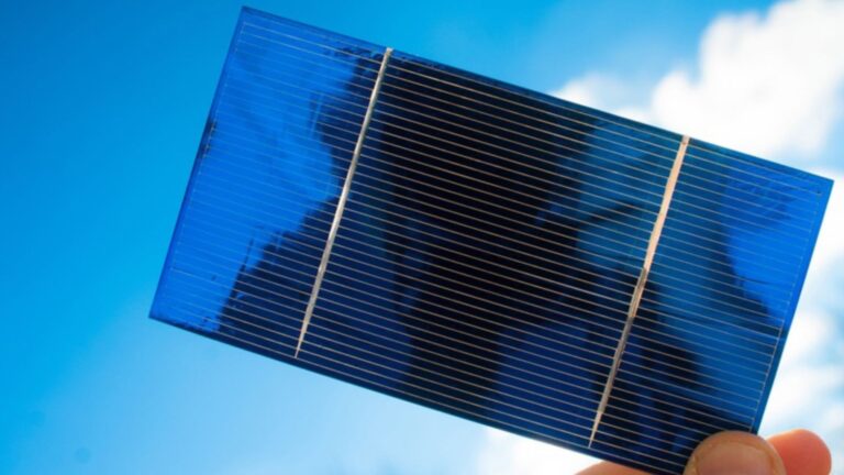
Researchers in Japan have developed a new solar cell with record performance using copper gallium selenide (CuGaSe₂), an indium-free semiconductor material.
The device achieved a power conversion efficiency of 12.28%, the highest reported for wide-bandgap chalcogenide solar cells in the 1.65–1.75 eV range.
The work was carried out by scientists at the National Institute of Advanced Industrial Science and Technology (AIST). The team focuses on next-generation solar technologies that could improve the efficiency of tandem solar cells.
CuGaSe₂ belongs to the chalcopyrite family of semiconductors and is closely related to the well-known Copper Indium Gallium Selenide used in thin-film solar panels. However, CuGaSe₂ has one major advantage. It does not require indium, a rare and expensive element.
READ ALSO: Trump’s Failed Superweapon Returns? US Navy Fires Railgun Again After Years
The material also possesses several properties that make it highly attractive for solar energy applications. It has a direct bandgap of about 1.68 eV, enabling efficient absorption of visible sunlight and improving energy conversion.
The material also features a high absorption coefficient, meaning that even very thin layers can capture a large portion of incoming light.
In addition, it demonstrates strong defect tolerance, enabling the solar cell to maintain good performance even when the crystal structure contains imperfections. These characteristics make it a promising candidate for advanced thin-film solar technologies.
Lead researcher Shogo Ishizuka highlighted the importance of the achievement.
WATCH ALSO: Top research robot integrated with new intelligence platform
“We regard this efficiency as the highest reported for wide-bandgap chalcogenide solar cells in the 1.65–1.75 eV range, particularly among indium-free chalcopyrite solar cells,” Ishizuka said.
He added that the result surpasses earlier CuGaSe₂-aluminum solar cells listed in the latest efficiency tables published in the journal Progress in Photovoltaics.
The device’s performance was independently verified by the photovoltaic calibration and measurement team at AIST’s Renewable Energy Advanced Research Center.
The new solar cell builds on an earlier design developed by AIST researchers in 2024.
Scientists introduced aluminum engineering in the backside region of the CuGaSe₂ film. This created a back-surface field (BSF) that improves the movement and collection of electrical charges.
The improved design significantly enhanced several key performance parameters of the solar cell. The device achieved a power conversion efficiency of 12.28%.
READ ALSO: Meet HON6000: Honeywell’s New Engine Designed for Future Autonomous Warplanes
It marks the highest reported performance for this type of indium-free wide-bandgap chalcogenide solar cell. It also recorded an open-circuit voltage of 0.996 volts, indicating stronger voltage output from the device.
In addition, the cell delivered a short-circuit current density of 17.90 mA/cm², reflecting efficient generation of electrical current from absorbed sunlight. The device also reached a fill factor of 68.8%, which measures how effectively the solar cell converts generated charge into usable electrical power.
These improvements demonstrate better overall device performance and energy conversion capability.
By comparison, the previous device achieved 12.25% efficiency with slightly lower voltage and current.
Researchers also optimized the aluminum gradient within the absorber layer and used a thicker cadmium sulfide (CdS) buffer layer to reduce energy losses due to recombination at material interfaces.
The solar cell was built using a layered thin-film structure designed to efficiently capture and convert sunlight into electricity. The device base is a soda-lime glass substrate that provides mechanical support.
On top of this, researchers deposited a molybdenum (Mo) layer that serves as the back electrical contact. Above the Mo layer is the CuGaSe₂ absorber layer, the main component that absorbs sunlight and generates charge carriers.
A cadmium sulfide (CdS) buffer layer is then added to form the p–n junction and improve charge separation. This is followed by a zinc oxide (ZnO) window layer that allows sunlight to pass while helping to conduct electricity.
READ ALSO: Artemis II Back on Track: NASA Targets April 1 Launch for First Crewed Moon Flight in 50 Years
Finally, a metal grid electrode is placed on the top surface to collect and transport the current generated by the solar cell.
The CuGaSe₂ absorber was grown using a three-stage deposition process, with aluminum and rubidium fluoride added during specific stages to control the material structure and electronic properties. Researchers also applied alkali post-deposition treatment to reduce defects and improve charge transport.
Step Toward Tandem Solar Cells
The team says the research is still at the fundamental development stage.
“Our work focuses on developing wide-bandgap devices for use as top cells in tandem solar cells,” Ishizuka said.
He explained that building a complete tandem system would require a compatible bottom solar cell and additional integration technologies.
WATCH ALSO: Two humanoid robots hold unscripted conversation for hours
“For now, this research is not yet ready for mass production,” he said. “A detailed cost analysis has not been carried out because the technology is still in the basic research phase.”
The study describing the record-setting device was published in the journal Science Advances under the title “Bulk and interface engineering of 1.7 eV–bandgap chalcogenide solar cells enabling record efficiency.”
The findings highlight the potential of indium-free thin-film solar technologies that could contribute to future high-efficiency tandem solar panels.