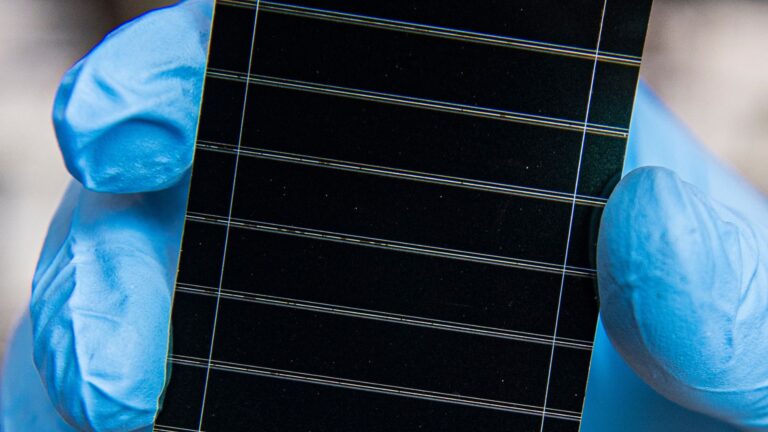
Scientists at the Xinjiang Technical Institute of Physics and Chemistry have cracked a decades-old barrier, cultivating a novel crystal that unleashes the world’s most powerful solid-state vacuum ultraviolet laser. Led by Institute Director Pan Shilie, the team’s ammonium fluorooxoborate (ABF) crystal generates a beam at a record 158.9 nanometres—the shortest wavelength ever achieved—with an energy output that dwarfs previous systems, all from a desktop-sized unit. This breakthrough directly tackles the need for compact, affordable, and high-performance light sources critical for everything from carving next-gen chips to powering space-based communications
For years, the quest for a more powerful, practical deep-ultraviolet laser has been a bit like searching for a mythical material. The goal? A solid-state crystal that could reliably produce an intense beam with a wavelength short enough to unlock new scientific and industrial frontiers. The existing champion, a crystal developed in the 1990s, had held its ground for decades. Now, as reported by the South China Morning Post, a Chinese team has not only found a new contender but has watched it shatter multiple world records in the lab.
The core problem this ABF crystal solves is surprisingly straightforward: how do you get a laser that’s simultaneously powerful, precise, compact, and affordable? For cutting-edge manufacturing and quantum research, the light sources have often been massive, complex systems like gas plasma chambers or synchrotrons that fill rooms and require immense energy and maintenance. The innovation from the Chinese Academy of Sciences promises to pack that same capability into a box on a table.
READ ALSO: https://modernmechanics24.com/post/china-self-powered-eye-tracker-als/
So, what does it actually do? At its most basic function, the ABF crystal acts as a super-efficient wavelength converter. You shine a relatively common infrared or visible laser into it, and through a process called direct frequency doubling, the crystal reliably outputs a concentrated beam of vacuum ultraviolet light. This isn’t just a color change; it’s a fundamental shift in capability. The resulting 158.9 nm laser beam carries much higher energy and allows for precision at an atomic scale, which is exactly what’s needed for etching ever-smaller semiconductor features or manipulating individual atoms for a quantum computer.
The mastermind behind this leap is innovator and research lead Professor Pan Shilie, who guided the theoretical design. The engineering feat of actually growing the crystal from a millimetre-sized seed to a viable centimetre-scale component was a ten-year marathon undertaken by his dedicated team at the institute. “The ABF crystal is a novel material, entirely developed and patented by our institute – from initial design to crystal growth, to final laser output,” Pan stated in an interview, underscoring the homegrown nature of this achievement.
WATCH ALSO: https://modernmechanics24.com/post/china-launches-80000-ton-fujian-aircraft-carrier/
The numbers, detailed in their Nature paper, are staggering. Beyond the headline-grabbing shortest wavelength, when tuned to 177.3 nm, the system delivered a pulse energy of 4.8 millijoules and a conversion efficiency of 7.9%—both global records for this type of laser. This efficiency is a big deal; it means less input energy is wasted, making the whole system more practical and powerful.
However, every breakthrough has its current boundaries. One honest limitation is the sheer maturity and scale of the crystal growth process. The team first synthesized the ABF compound in 2016, and scaling it up has been a decade-long challenge. Widespread commercial or industrial adoption will depend on further refining these growth and processing techniques to produce larger, even higher-quality crystals reliably and at volume. It’s a laboratory champion now, but the path to factory floors is still being paved.
READ ALSO: https://modernmechanics24.com/post/ammonia-innovation-food-economic-growth/
The overall value and summary of this work, however, points far beyond the lab bench. China is ambitiously moving from manufacturing giant to a high-tech powerhouse, and tools like this are the instruments of that transformation. “There are many fields where we need to lead and create demand, not simply follow behind the West,” Pan explained. This laser isn’t just for improving existing tools like spectrometers or lithography machines; it’s intended to create entirely new applications.
Imagine secure satellite networks communicating with beams of light that are completely absorbed by Earth’s atmosphere, making them impervious to ground-based interception. Or peer deeper into the mysteries of superconductivity, seeing details others miss. According to the SCMP report, these are the “uncharted territories” Pan’s team is eyeing. In quantum computing, such a precise and energetic laser is a dream tool for controlling qubits. In semiconductor manufacturing, it could define the circuitry for chips a generation or two ahead.
WATCH ALSO: https://modernmechanics24.com/post/us-supersonic-jet-cuts-flight-time-silences-sonic-boom/
The journey from a theoretical design to a record-holding beam of light encapsulates modern material science at its best. It’s a story of patience, precision, and a clear vision of technological sovereignty. The ABF crystal breakthrough isn’t just a new entry in a scientific record book; it’s a key that could unlock doors across physics, industry, and even the infrastructure of space itself.