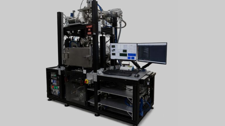
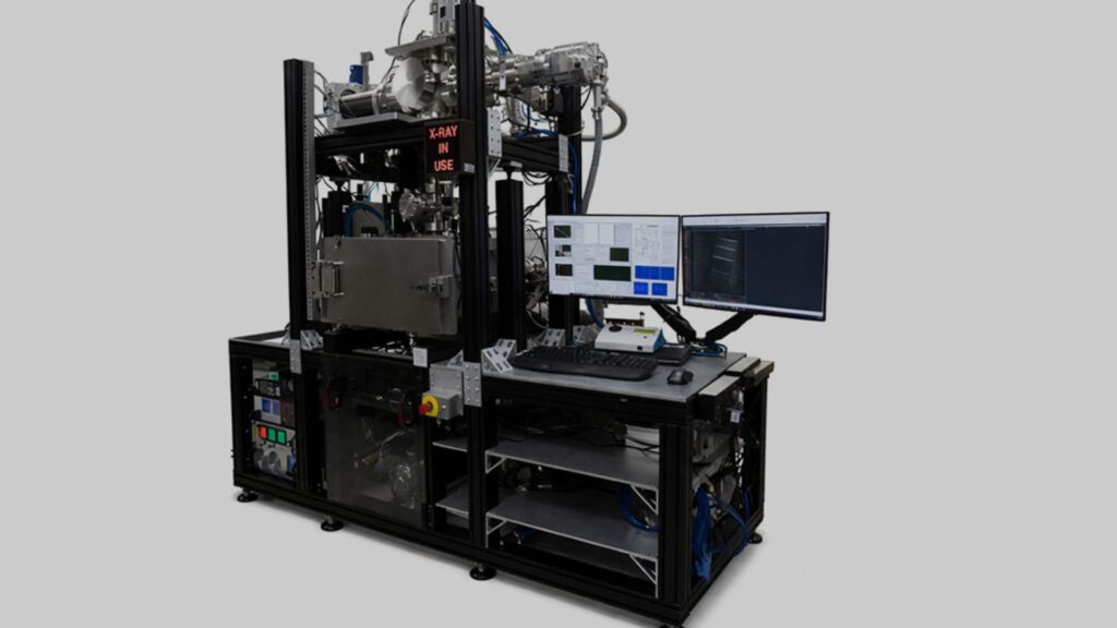
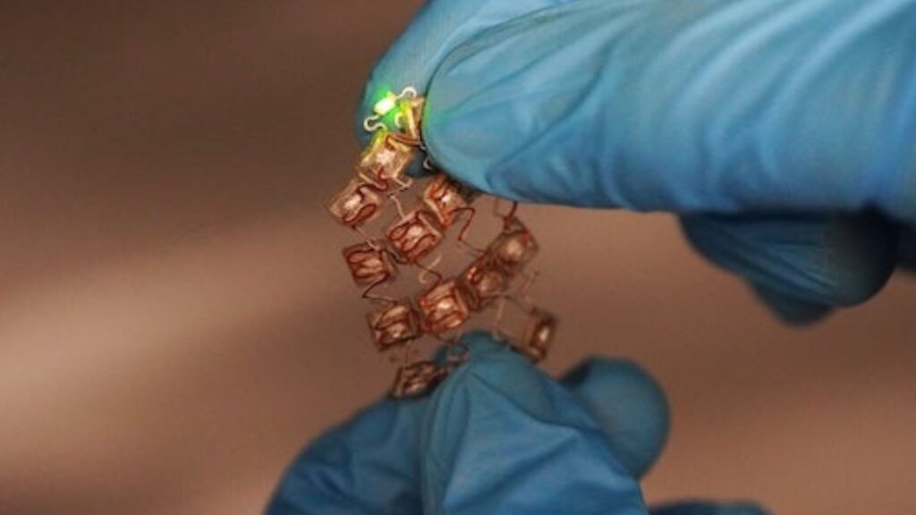
A U.S. academic and industry team has fabricated the first high-performance monolithic 3D computer chip in a domestic foundry, achieving a record density of vertical wiring and demonstrating speed improvements roughly ten times greater than conventional 2D chips. The breakthrough, led by Professor Subhasish Mitra of Stanford University, offers a tangible path to overcoming the crippling data bottlenecks in modern AI hardware.
Imagine the difference between navigating a sprawling suburb versus a vertical city with high-speed elevators. For the data powering AI models like ChatGPT, that’s the leap forward promised by a new 3D chip developed by researchers from Stanford University, Carnegie Mellon University, the University of Pennsylvania, and MIT. In collaboration with the U.S.-based foundry SkyWater Technology, the team has built a prototype that stacks computing and memory layers like stories in a skyscraper, a feat reported by Stanford News that could redefine the future of American semiconductor innovation.
READ ALSO: https://modernmechanics24.com/post/turkey-mine-clearing-system-400kg-rocket/
The fundamental problem plaguing today’s flat chips is what engineers call the “memory wall.” AI requires shuttling enormous amounts of data between memory and processors. On a 2D chip, these components are spread apart, connected by only a few crowded, slow pathways. The processors end up idling, waiting for data to arrive. For decades, the industry smashed through this wall by making transistors smaller and packing more onto a chip, but that strategy is now hitting the “miniaturization wall” of physics.
“The memory wall and the miniaturization wall form a deadly combination,” said Robert M. Radway, assistant professor at the University of Pennsylvania, a co-author on the study. This new research, he explained, attacks it head-on by building upward. Instead of placing components side-by-side, they are stacked directly on top of each other, connected by a dense network of vertical nanowires that act as ultra-fast data elevators. This monolithic 3D approach, where layers are built sequentially in one process, allows for connections that are orders of magnitude denser than stacking pre-made chips.
The significance isn’t just in the design but in its proven manufacturability. “Turning a cutting-edge academic concept into something a commercial fab can build is an enormous challenge,” stated co-author Mark Nelson, Vice President at SkyWater Technology. He emphasized to Stanford News that this demonstrates advanced architectures can be produced domestically and at scale, which is critical for U.S. technological leadership. The prototype, fabricated entirely at SkyWater, already shows a four-fold performance gain over comparable 2D chips in early tests.
WATCH ALSO: https://modernmechanics24.com/post/us-supersonic-jet-cuts-flight-time-silences-sonic-boom/
Simulations of more advanced versions with additional stacked layers are even more promising, showing potential for up to a twelve-fold improvement on real AI workloads and a path to improving the critical energy-delay product by a staggering 100 to 1,000 times. This means future chips could be both radically faster and far more energy-efficient.
“This opens the door to a new era of chip production and innovation,” said lead researcher Subhasish Mitra, the William E. Ayer Professor at Stanford. He framed the work as essential groundwork for the massive hardware leaps future AI will require. The research was presented at the prestigious 71st Annual IEEE International Electron Devices Meeting (IEDM).
Beyond raw metrics, the project seeds a vital domestic capability. Just as the integrated circuit revolution was fueled by U.S.-trained engineers, this work, supported by initiatives like the Microelectronics Commons Northwest AI Hub, is training a new generation in 3D integration. As H.-S. Philip Wong, the Willard R. and Inez Kerr Bell Professor at Stanford, noted, such breakthroughs are about more than performance—they’re about reclaiming the capability to shape the foundational hardware of the AI age.
READ ALSO: https://modernmechanics24.com/post/worlds-largest-spider-web-110000-spiders-2/